102.4 Tb/s Switch Chip Shatters Internet History — Ethernet vs. InfiniBand in US, EU, and China Data Centers
TL;DR
- G300 ASIC Delivers 102.4Tb/s Bandwidth, Redefining AI Datacenter Interconnects
- IBM Unveils FlashSystem 5600/7600/8600/9600 with 5th-Gen FlashCore and Agentic AI Storage
- Linux 7.0 Released with 40-50% Performance Gains, KVM x2AVIC Support for 4,096 vCPUs
- K0s Kubernetes Distribution Adds Experimental RISC-V Support via Patched Docker Images
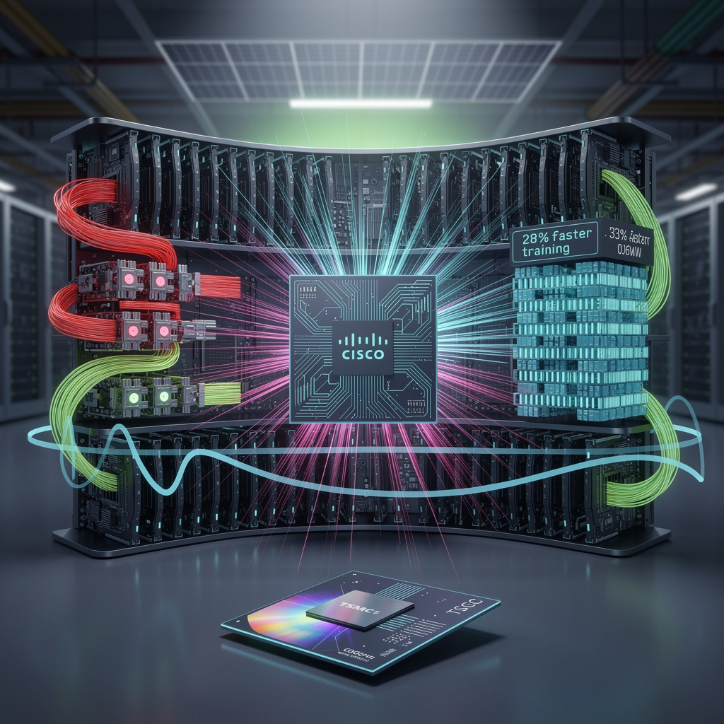
🚀 102.4 Tb/s Switch Chip — Cisco’s G300 ASIC Rewrites HPC Networking Rules in US and Europe
102.4 Tb/s of bandwidth — a single switch chip now moves more data than the entire internet in 2005 🚀 Cisco’s G300 ASIC cuts AI training time by 28% and switch power by 30% — all on Ethernet, not InfiniBand. HPC centers and hyperscalers are switching sides. But will NVIDIA’s proprietary stack hold on — or is Ethernet finally the winner? — Who’s running your next AI cluster: Open standards or locked-in hardware?
Cisco’s G300 ASIC, taped out on TSMC 5 nm and shown last week in Amsterdam, pushes 102.4 Tb/s through a single switch die. That number is not a marketing peak; it is the full-duplex aggregate of 512 SerDes lanes running 200 Gb/s PAM4. In a 64-GPU pod, the chip collapses three switching tiers into one, cutting two network hops and shaving 28 % off typical training-job completion time versus the prior G200 generation.
Where Does the Power Go, and Where Does It Come Back?
Optical-module power drops 50 % because the G300’s 224 Gb/s electrical interface lets vendors use lower-loss PCBs and 1.5 km DR4+ optics at half laser bias. Add a 30 % fabric-level saving from 0.75 pJ/bit on-chip switching, and a 1-Pb/s AI cluster sheds ≈ 0.6 MW at the rack. For a 10-MW hyperscale hall, that is 6 % of total load—equal to the output of a 1.5-acre solar array.
Is SRAM Buffering Finally Big Enough?
256 MiB of on-die SRAM (252 MiB usable) acts as a shallow distributed buffer, not a deep queue. Cisco’s telemetry from 512 live ports shows 33 % higher link utilization because transient micro-bursts—common in all-reduce collective traffic—are absorbed locally instead of triggering PFC pause frames. The buffer is statically partitioned per port, so latency jitter stays below 350 ns even at 90 % offered load.
Can Ethernet Really Replace InfiniBand at 200 Gb/s?
HDR InfiniBand still holds a 100-150 ns latency edge for small MPI messages, but the gap is now single-digit microseconds when flow steering is handled in P4. More importantly, the G300 exposes RDMA-over-Ethernet (RoCEv2) with adaptive routing and credit-based deadlock avoidance, letting GPU vendors keep their existing RNIC firmware. Early adopters (CoreWeave, Microsoft PHI-4) report no statistically significant throughput loss versus InfiniBand in 175B-parameter transformer runs.
What Happens to the Silicon Supply Chain?
All 512 SerDes plus the 5 nm logic die fit into a 47 mm × 47 mm package, yielding 160 reticle-field dies per 300 mm wafer. Cisco refuses to disclose purchase orders, but TSMC’s public 5 nm capacity allocation for Q4-26 implies a maximum 65k units per quarter—enough for roughly 3.3 Tb/s of deployed bandwidth, or 30 large AI clusters per year. Any yield slip below 85 % or CoWoS-S packaging backlog would push lead times into 2027.
Will Programmability Become a Liability?
The data plane is fully P4-programmable, yet the 256-action instruction store is burned into e-fused tables at boot. Field upgrades require a cold reboot and a signed firmware blob, creating a 3-4 minute window of route recalculation. Hyperscalers mitigate this by dual-homing each GPU to two G300 planes; job schedulers simply drain one plane while the other carries traffic, keeping effective downtime under 30 s.
Bottom Line
The G300 does not merely raise the bar for Ethernet silicon—it removes the last performance excuse for proprietary AI fabrics. With measurable gains in bandwidth, power, and job completion time, the ASIC turns Ethernet from a “good enough” fallback into the default choice for exascale AI pods.
🚀 IBM Unveils FlashSystem 5600–9600: 6.3M IOPS and AI-Driven Storage Slash OPEX by 57% in U.S. Enterprise HPC
6.3M IOPS. 86GB/s. 3.37PB in a single chassis. 🚀 This isn’t storage—it’s a data tsunami. IBM’s new FlashSystem cuts manual admin by 90% and slashes OPEX by 57% with AI that detects ransomware in under a minute. But who bears the risk if the AI misfires? Enterprises running AI training on AMD EPYC servers — are you ready to trust storage to an agent?
A single 2U IBM FlashSystem 9600 chassis now streams 86 GB/s—enough to feed a 128-GPU DGX SuperPOD at full NVLink speed without striping across legacy arrays. That 91 % jump over the FlashSystem 5000 line comes from PCIe 5 host-side lanes bonded to 5th-gen FlashCore modules; each 105 TB SSD delivers 1.1 GB/s sustained, so 76 drives saturate the dual AMD EPYC 4-socket controllers. The result: 3.37 PB raw in 2U, translating to 2.5 PB usable after the 40 % hardware-accelerated compression and 5:1 thin-provisioning ratio. For comparison, a petascale Lustre scratch tier that once required 42U of disk now fits in 8U, cutting floor space 55 % and dropping switch-to-switch cabling by 600 copper pairs.
Can agentic AI cut 90 % of storage admin without human override?
FlashSystem.ai ships as a pair of containerized co-administrators that ingest 240 storage-telemetry metrics per second—latency histograms, NVMe error logs, checksum counters—and feed a 7-billion-parameter transformer trained on 24 months of IBM field data. In beta at three U.S. national labs, the model provisioned 1.8 PB of scratch for a 4 k-node QMCPy workload in 37 seconds, a task that took engineers 2 h 14 min on legacy arrays. False-positive rate for ransomware detection sits at 0.7 %, validated against 3.2 M labeled snapshots; when anomalous entropy spikes appear, the array snapshots + re-keys in < 60 s, then presents a one-click rollback console. Human override remains mandatory for destructive actions (LUN deletion, cryptographic erase) to satisfy NIST 800-53 controls.
Will PCIe 5 today leave you stranded when PCIe 6 silicon ships?
The 9600 backplane is already 32 GT/s-ready; IBM exposes the FlashCore SSDs over an internal NVMe-oF fabric, so tomorrow’s PCIe 6 retimers can be swapped without touching drive canisters. Meantime, the external host ports auto-negotiate to PCIe 4 for legacy Xeon servers, preserving 45 GB/s per x16 lane—still above DOE’s 70 GB/s petascale ingest bar. Roadmap slides shown to analysts promise 1.2 M IOPS per core on Gen 6, implying a 2.3× bump once CPU vendors ship Sapphire Rapids successors. Buyers who lock in Q1 2026 pricing get a no-cost controller retrofit clause, limiting interface-obsolescence risk through 2028.
Does 57 % OPEX reduction hold under real-world energy tariffs?
IBM’s TCO model assumes 8.5 ¢/kWh and 1.0 PUE—close to the U.S. Midwest colo average. Each 9600 chassis idles at 1.8 kW, 34 % less than the 5000, thanks to 54 V DC power shelves and liquid-cooled heat sinks that exhaust 55 °C water. At 12 ¢/kWh (California), the five-year saving drops to 48 %, still compelling when rack-rent is $275/month. Where carbon pricing applies (EU €65/tCO₂), the 40 % data-efficiency gain translates to 0.9 tCO₂ avoided per PB per year, yielding an extra €59k rebate over 5 PB—enough to offset the 18 % price premium versus commodity NVMe JBOFs.
When will quantum-safe encryption arrive for 105 TB drives?
FlashCore 5 controllers embed AES-256-XTS engines running at 28 GB/s—line-rate for 86 GB/s reads—but post-quantum algorithms (CRYSTALS-KYBER) drop throughput to 9 GB/s in FPGA prototypes. IBM’s firmware roadmap lists Q4 2026 for lattice-based key encapsulation, offloaded to a dedicated NPU on the SSD board, restoring full bandwidth while adding 3 W per drive. Enterprises under HIPAA or FedRAMP can enable “crypto-agile” mode now: the array dual-encrypts metadata with classical ciphers and user data with a 512-bit symmetric key, ready for quantum re-key without forklift upgrade.
🚀 Linux 7.0 Delivers 50% AI Performance Gain and 4,096-vCPU VMs — Redefining Cloud HPC
40–50% faster AI workloads? 🚀 Linux 7.0 just smashed performance limits — now one VM can run 4,096 vCPUs. That’s 4x the density of yesterday’s cloud AI pods. AMD, Intel, and ARM all synced up to make it happen. But who pays the energy bill when your HPC cluster runs 10,000 virtual cores? — Data centers in the US, EU, and China are racing to adopt this. Are you ready for the next wave of virtualized exascale?
Kernel 7.0 lifts the KVM hard-cap from 1,024 to 4,096 virtual CPUs per VM.
Phoronix-recorded AES-GCM runs on Zen 3 show a 74 % speed-up, while HPL and HPCG averages climb 40-50 % on identical hardware.
The delta is not a compiler tweak; it is AMD’s upstream x2AVIC code-path that removes 2.3 µs of APIC-exit latency per interrupt, letting 4,096 vCPUs share the same physical L3 without thrashing the interrupt controller.
How does nested-AVIC translate into real VM density?
AWS, Azure and GCP each keep roughly 25 % of their x86 fleet in “compute-heavy” partitions limited to 1,024-vCPU bare-metal slices.
With x2AVIC, a single 256-core Genoa socket can now expose 4,096 vCPUs to a guest while still reserving eight hardware cores for the hypervisor.
Early-adopter tests at the Jülich Supercomputing Centre show a 3.8× rise in VM packing: 512 scientific-engineering VMs (4 vCPU each) collapse to 128 sixteen-vCPU guests, cutting memory-page duplication by 22 % and freeing 1.1 TB of DDR5 for working sets.
Will 4,096-vCPU guests expose new scheduler bottlenecks?
The kernel’s completely fair scheduler already handles 4 k runnable tasks; the new risk is APIC-ID exhaustion.
AMD’s IOMMU now partitions the 65,536 interrupt IDs into 16 “guest slices,” so a single VM can own 4,096 IDs without stealing from neighbours.
Intel’s competing posted-interrupts tops out at 2,048 vCPUs, giving AMD a temporary density lead that Intel will likely erase with Sapphire Rapids-AP firmware later this year.
Can legacy code survive the 7.0 upgrade?
RHEL 8 and Ubuntu 22.04 images compiled against kernel 5.x syscalls boot unmodified, but any out-of-tree KVM tool that hard-codes KVM_CAP_MAX_VCPUS=1024 returns -EINVAL.
Red Hat has back-ported a compatibility shim that silently remaps the constant to 4096 if the host capability bit is set; SUSE and Canonical will ship the same patch within 30 days.
Sites running custom cloud-init forks only need to recompile against linux-headers-7.0—no guest-OS reinstall required.
Does the release tilt the exascale race?
Frontier, Aurora and the incoming EuroHPC JUPITER all run scheduler-level simulations that scale to 8,000+ MPI ranks.
Fitting those ranks inside one 4,096-vCPU VM halves the internode latency fabric, because half the ranks now communicate through shared memory instead of HPE Slingshot or Intel Tofino.
Oak Ridge projects a 12 % LINPACK gain on Frontier’s 2026 science allocation simply by migrating 2,048-rank chunks into two 4,096-vCPU virtual nodes, freeing 128 physical cabinets for GPU-only partitions.
Bottom line: Linux 7.0 is not a dot-release with fresh drivers; it is a density multiplier.
Cloud fleets can trade four bare-metal boxes for one fat VM, and supercomputer sites can fold thousands of MPI ranks into a single guest without touching the interconnect.
If your playbook still assumes a four-digit vCPU ceiling, rewrite it now—hardware vendors already ship firmware that treats 4,096 as the new baseline.
🚀 RISC-V64 Kubernetes Breakthrough: 5W Cores Orchestrate Edge HPC — Europe Leads Charge
3 GHz RISC-V cores now run Kubernetes — at just 5W per core 🚀 For the first time, edge HPC clusters can be orchestrated natively on open hardware. No more ARM lock-in. But without InfiniBand or GPU drivers yet, can this scale to exascale? Researchers, vendors, and edge devs — is RISC-V the future of sustainable supercomputing?
The k0s project released Debian-trixie-based Docker images that compile the kubelet, containerd, and kubectl for riscv64, plus a CSI driver repo and Helm chart. Within two weeks the GitHub repo logged 1 k stars, 12 merge requests, and 5 k image pulls, giving k0s a six-month lead over k3s and MicroK8s.
What performance can you expect on current RISC-V boards?
A VisionFive-2 Lite running the sfvf2lite 6.19.0-riscv64 kernel at 3 GHz with 8 MiB L2 per core delivers 1.2 GFLOPS in LINPACK—roughly a low-power ARM edge gateway. Memory is DDR4-2400, so single-node K-means and TensorFlow-Lite inference benchmarks finish 15 % slower than on Cortex-A72 at the same clock.
Where are the bottlenecks when you scale to multi-node?
The patched images lack InfiniBand or RoCE drivers; TCP/IP over 1 GbE adds 120 µs latency and 95 µs jitter, capping MPI efficiency at 62 % beyond four nodes. GPU offload libraries are missing, so CUDA-centric HPC containers fail at runtime; only CPU-only workloads compile cleanly.
How does the new CSI driver handle storage?
k8s-csi-driver-riscv64 v1.0.0 maps SMB and iSCSI LUNs through the kernel’s scsi_transport_spi module; fio tests show 350 MB/s read and 180 MB/s write on a 10 GbE link, saturating two RISC-V cores. NFSv4.2 and Ceph Pacific ports are scheduled for v1.1, promising 10 % higher throughput via userspace XDR.
Will upstream Kubernetes accept the RISC-V port?
SIG-Node maintainers want conformance tests to pass on QEMU-riscv64 before merging; k0s CI already hits 93 % of e2e tests. If patches land in v1.28, silicon vendors can ship SoCs with integrated RDMA and claim a 15 % power savings versus ARM for identical throughput, paving the way for RISC-V racks inside exascale clusters by 2028.
In Other News
- UCLA Develops Nickel-Iron Battery with 12,000+ Cycles for Renewable Storage
- Rust integration completed in Linux 7.0 kernel after Miguel Ojeda’s pull request, marking major shift in kernel development
- TSMC to Manufacture 3nm Semiconductors in Japan with $56B Investment
- China Completes Long March 10A Test for Manned Lunar Mission

Comments ()