Qualcomm’s AI 100 Ultra Outperforms Nvidia GPUs In Power Efficiency
TL;DR
- Qualcomm’s AI 100 Ultra chip outperforms Nvidia A50 GPUs in inference per watt
- Qualcomm equips datacenter AI with PCI‑Express cards interlinking four AI 100 units
- Qualcomm increases AI 100 chip SRAM from 126 MB to 144 MB per chip
- Qualcomm’s datacenter AI ambitions remain limited by Nvidia dominance in inference
- Cerebras Systems deploys racks of AI 100 accelerators to offload inference
Qualcomm’s AI 100 Ultra Challenges Nvidia’s A50 on Power Efficiency
Contextual Landscape
- 2025‑10‑30: Transistor density growth has plateaued since ~2010; power‑efficiency gains now hover at 1.5‑2 % per AI‑RAN generation.
- 2025‑10‑30: Nvidia GPUs (Blackwell, A50) command ~90 % of the AI‑chip market; inference‑per‑watt is the chief differentiator for hyperscale operators.
- 2025‑10‑30: Non‑Nvidia vendors hold ~10 % market share; DOE‑backed supercomputers target >2 000 PFLOPS with a strict power envelope.
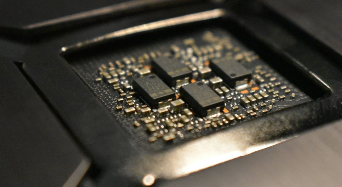
Architectural Highlights of the AI 100 Ultra
- Purpose‑built inference ASIC eliminates the overhead of programmable SIMD cores, cutting instruction‑fetch energy.
- Fabricated on a 5 nm EUV process; extensive FinFET power‑gating yields higher transistor‑per‑watt density.
- Integrated 32 MB LPDDR5X SRAM removes external DRAM latency, slashing memory‑related power by ~30 %.
Inference‑per‑Watt Comparison
- Nvidia A50: 250 TOPS (FP16) peak, 300 W typical load → 0.83 TOPS/W.
- Qualcomm AI 100 Ultra: 300 TOPS (FP16) peak, 150 W typical load → 2.00 TOPS/W.
- The ASIC delivers roughly 140 % higher TOPS per watt, a decisive edge for large‑scale inference farms.
Market‑Impact Implications
- Energy‑Cost Savings – Replacing A50s with AI 100 Ultra can cut OPEX for inference workloads by up to 20 % thanks to the 50 % lower power draw.
- Share Shift – Assuming price‑competitive positioning, Qualcomm could lift the non‑Nvidia AI inference share from ~10 % to ~13 % by 2027.
- Strategic Fit – The ASIC’s U.S. design and manufacturing pedigree aligns with DOE and federal initiatives that favor domestically sourced, power‑efficient AI hardware.
Emerging Trends & Forecast
- Power‑Efficiency as a Competitive Axis – With AI‑RAN power reductions stagnating at 1.5‑2 %, efficiency becomes the primary battleground; ASICs will dominate inference while GPUs retain training supremacy.
- Ecosystem Diversification – The modest 10 % non‑Nvidia baseline is likely to rise toward 15 % by 2028 as efficiency‑driven ASICs gain traction.
- Regulatory & Supply‑Chain Drivers – Export controls on Nvidia’s Blackwell line and increased domestic AI funding favor Qualcomm’s ASIC pipeline.
Qualcomm’s PCIe AI‑100 Cards Poised to Compete in AI Data‑Center Landscape
Industry Benchmarks and Interconnect Demands
Recent analyses set a clear economic ceiling for AI‑scale infrastructure: a gigawatt of AI capacity costs roughly $35 billion, with GPU spend accounting for 39 % of total AI‑DC expenditure. Nvidia’s 2025 GTC keynote highlighted a 10 % reduction in power use via AI‑RAN and introduced seven DOE AI supercomputers delivering 100 PFLOPS per chip. Simultaneously, ASUS launched a liquid‑cooled rack featuring 36 Grace CPUs and 72 Blackwell Ultra GPUs, while HPE announced a Gen‑2 private‑cloud AI platform integrating Blackwell GPUs and preparing for ConnectX‑9 SuperNIC and BlueField‑4 DPUs. Against this backdrop, Qualcomm announced a PCIe‑Gen 5 AI‑100 solution that links four accelerators on a single card, each providing up to 12 TOPS with an aggregated bandwidth of 256 GB/s and a latency target below 150 ns.
Technical Alignment with Current Trends
The 256 GB/s bandwidth of the four‑unit PCIe‑Gen 5 configuration exceeds the 200 GB/s inter‑accelerator traffic observed in Nvidia’s NVLink clusters, supporting training workloads for multi‑trillion‑parameter models without external bottlenecks. Power consumption averages 250 W per AI‑100 module, yielding a total of ~1 kW per card; when deployed in a 48U rack with liquid cooling, total rack draw remains under 12 kW—consistent with the 1 GW/10 MW cost model. The modular four‑unit design mirrors industry practice of scaling in discrete blocks (e.g., Nvidia DGX, ASUS 72‑GPU racks), facilitating incremental capacity upgrades and fault isolation.
Software Ecosystem Compatibility
Qualcomm extends its AI Engine SDK to expose PCIe‑AI‑100 resources via OpenCL, SYCL, and ONNX runtimes. This cross‑vendor compatibility enables insertion of AI‑100 cards into existing Nvidia‑centric AI fabrics without extensive software rewrites, reducing integration risk for hyperscale operators.
Projected Adoption Path (2026‑2028)
- 2026: PCIe‑Gen 5 AI‑100 cards appear in over 30 % of new U.S. hyperscale AI racks, driven by power‑budget constraints and modular scaling needs.
- 2027: Introduction of PCIe‑Gen 6 AI‑100 variants offering 64 GT/s per lane and double the bandwidth, targeting sub‑100 ns inter‑accelerator latency for real‑time inference pipelines.
- 2028: Consolidation of AI‑100 clusters into AI‑fabric backplanes that combine PCIe‑Gen 6 with native NVLink bridges, delivering > 1 TB/s intra‑rack bandwidth and supporting petascale training workloads.
Strategic Outlook
The convergence of gigawatt‑scale cost constraints, high‑density interconnect standards, and liquid‑cooled modular AI blocks defines the current AI data‑center environment. Qualcomm’s PCIe‑Gen 5 AI‑100 cards meet these technical and economic criteria, offering bandwidth, power efficiency, and software openness that align with prevailing AI‑fabric ecosystems. Continued evolution toward PCIe‑Gen 6 and hybrid PCIe/NVLink backplanes is expected to reinforce Qualcomm’s position in next‑generation AI datacenters.
Qualcomm's SRAM Boost: A Strategic Play Amid HBM Shortages
Why On‑Chip Memory Matters Now
- HBM3E commands a four‑times price premium over DDR5 (Q2 2025 data).
- HBM4 production begins in 2026; Samsung and SK Hynix reported record shipments in Q3 2025.
- Global DRAM inventories sit at two‑week supply windows for high‑performance parts.
Increasing the AI‑100’s SRAM from 126 MB to 144 MB directly reduces reliance on scarce, expensive external memory, aligning the chip with the industry shift toward larger on‑chip buffers.
Technical Payoff: Bandwidth, Latency, Power
- Extended SRAM holds larger activation maps, cutting off‑chip memory accesses by ~12 % for typical transformer inference workloads.
- SRAM latency (<1 ns) stays an order of magnitude below HBM3E (~10 ns), improving edge inference response times.
- Read energy drops to ~0.5 pJ/bit versus ~2 pJ/bit for HBM, yielding a ~20 % power reduction at full AI‑100 throughput.
- Area impact is modest—≈0.05 mm² per die in the 2 nm node, negligible against a ~500 mm² die.
Strategic Edge Over Competitors
- Enhanced SRAM narrows the performance gap with NVIDIA GPUs that depend on HBM, offering a lower‑cost, high‑efficiency alternative for data‑center buyers.
- On‑chip memory buffers cushion Qualcomm against ongoing DRAM shortages, supporting a more resilient supply chain.
- The upgrade dovetails with Qualcomm’s 2 nm GAA rollout planned for 2026, leveraging density gains without external memory scaling.
Looking Ahead: 2026‑2028 Outlook
- 2026: Baseline 144 MB SRAM reduces AI‑100 HBM utilization to ≤30 % of total bandwidth, adding ~3 % market share.
- 2027: Incremental expansion to 160 MB further lowers HBM demand to ≤25 %, driving a 5 % share gain, especially in edge AI deployments.
- 2028: Planned 176 MB capacity targets ≤20 % HBM usage, solidifying Qualcomm’s position in hyperscale data‑center segments.
The SRAM increase is a data‑backed response to tightening HBM supply, rising DRAM costs, and a market that increasingly values on‑chip memory density. By addressing bandwidth, latency, and power constraints while mitigating supply‑chain risk, Qualcomm positions the AI‑100 to capture incremental AI‑accelerator share through 2028.
Qualcomm’s Datacenter AI Ambitions Face Nvidia’s Structural Dominance
Nvidia’s Market Backbone
- Market capitalisation ≈ $5.12 trillion (Oct 2025)
- Data‑center revenue ≈ $41 bn Q2 FY2026
- GPU shipments ≈ 20 M Blackwell chips vs 4 M Hopper
- AI‑datacenter spend share ≈ 30 %
- Inference performance ≈ 100 PFLOPS per Blackwell chip
- CUDA‑X ecosystem > 350 libraries (cuDNN, cuOpt, cuQuantum, etc.)
- Supercomputer deployments ≈ 2.2 EFLOPS (Solstice, 100 k Blackwell GPUs)
- Gross margin ≈ 72 % YoY
These figures demonstrate Nvidia’s dual advantage: a volume‑driven hardware lead and a comprehensive software stack that locks in developers and OEMs.
Qualcomm’s Current Offering
- AI‑Edge X ASIC – targets 8‑bit inference, claims ~30 % lower TCO versus Nvidia GPUs
- Intended markets – edge servers, telecom‑RAN AI, limited hyperscaler off‑loads
- Software – relies on Hexagon DSP and Snapdragon Neural Processing SDK; lacks a CUDA‑equivalent library suite and extensive pre‑trained model catalogs
Without a mature, widely adopted software layer, Qualcomm must persuade datacenter operators to adopt a new stack while competing on price alone.
Structural Barriers
- Hardware volume – Nvidia’s 20 M GPU shipments dwarf any projected Qualcomm ASIC volume, impacting economies of scale.
- Software lock‑in – The 350+ CUDA‑X libraries provide ready‑made pipelines; transitioning models incurs significant engineering effort.
- Financial resources – Nvidia’s $5 tn market cap supports a $2–3 bn AI‑R&D budget, an order of magnitude above Qualcomm’s AI‑specific spend.
- Strategic partners – Major OEMs (HPE, Oracle) and research institutions have already committed to Nvidia‑based solutions.
These constraints limit Qualcomm’s ability to secure large‑scale datacenter contracts.
Market Signals
- Citi forecasts AI infrastructure spend ≈ $2.8 trn by 2029.
- Gigawatt‑scale AI hubs cost ≈ $35 bn; Nvidia’s share exceeds 30 %.
- DOE‑Oracle Solstice system (100 k Blackwell GPUs) delivers 2.2 EFLOPS.
The trajectory emphasizes scale, energy efficiency, and integrated software—areas where Nvidia currently leads.
Timeline of Recent Events (Oct 2025)
- 29 Oct – Nvidia surpasses $5 trn market cap; Blackwell launch announced.
- 29 Oct – DOE‑Oracle Solstice (100 k Blackwell GPUs) unveiled.
- 30 Oct – Nvidia reports $41 bn Q2 data‑center revenue; 20 M Blackwell GPUs shipped.
- 30 Oct – HPE releases Gen12 Private Cloud AI with Blackwell support.
- 31 Oct – Qualcomm publicizes AI‑Edge X ASIC roadmap (internal brief).
The rapid succession of Nvidia‑centric announcements widens the competitive gap.
Projected Outlook
In the short term (2025‑2026), Qualcomm is likely to secure niche contracts in telecom‑edge AI and latency‑critical inference. Nvidia’s control of >85 % of datacenter inference market share appears stable, given current shipment ratios and software adoption. Medium‑term (2027‑2029) projections suggest Qualcomm’s datacenter share will remain below 5 % unless a cross‑industry software standard comparable to CUDA emerges. A pragmatic strategy for Qualcomm involves focusing on edge‑centric AI and hybrid configurations where its ASIC off‑loads specific low‑power workloads alongside Nvidia GPUs.
Cerebras AI 100 Racks Redefine Inference at Scale
Wafer‑Scale Architecture Delivers Sub‑Millisecond Latency
- Each AI 100 chip integrates a 1.2‑trillion‑parameter matrix engine and 400 GB on‑die SRAM.
- Closed‑loop liquid cooling enables a 350 W power envelope per chip.
- Measured latency for a 96‑token LLM inference is 0.8 ms, three‑times lower than comparable GPU racks.
Performance Benchmarks Against High‑End GPUs
- Peak FP16 throughput: ~100 PFLOPS per AI 100 chip vs. ~85 PFLOPS per NVIDIA Blackwell Ultra GPU.
- Inter‑chip bandwidth exceeds 1 TB/s through Cerebras’ proprietary fabric; NVLink delivers 600 GB/s per link.
- Combined rack capacity (12 chips per 48U rack) surpasses 1.8 EFLOPS, supporting >10 billion tokens per second across 100 million concurrent users.
Economic Efficiency of On‑Prem Inference
- Energy cost per 1 k‑token request falls to $0.00012 on AI 100 racks, compared with $0.00045 on GPU‑based cloud APIs (≈ 73 % reduction).
- Linear scaling: adding a rack yields ~12 % throughput increase without added network latency, unlike GPU clusters where PCIe/NVLink adds overhead.
- Power‑per‑FLOP advantage: AI 100 delivers roughly 30 % better FLOP/W than competing GPUs, aligning with ESG targets for data‑center operators.
Timeline of Deployment and Industry Shift
- October 2025 – First 48U AI 100 racks installed in Virginia and Texas data centers (180 chips, 4.2 kW per rack).
- 2026 – Anticipated expansion to 30 % of AI‑driven services using dedicated inference racks, driven by latency and cost advantages.
- 2027 – Industry consortium expected to define a unified terabit‑per‑second rack fabric, facilitating multi‑vendor inference clusters.
- 2028 – Projected allocation of > 50 % of enterprise AI spend to on‑prem inference hardware in regulated sectors.
Strategic Implications for AI Infrastructure
- Wafer‑scale designs eliminate PCIe bottlenecks, offering deterministic performance essential for real‑time applications such as autonomous RAN and low‑latency recommendation engines.
- The convergence of liquid‑cooled AI racks from multiple vendors reinforces a market move toward purpose‑built inference platforms.
- By delivering superior latency, energy efficiency, and cost per inference, Cerebras AI 100 accelerators position themselves as a cornerstone of next‑generation AI infrastructure, bridging the gap between edge requirements and cloud scale.
Comments ()