30% Throughput, 40% Latency Cut: Wi‑Fi 8 Arrives With 6GHz Spectrum and AI-Native Silicon
TL;DR
- Wi‑Fi 8: 30% Faster, 40% Lower Latency, 60% Cheaper Spectrum—The Wireless Revolution. Is your network ready for Wi‑Fi 8's 30% faster speeds and 60% cheaper spectrum?
- 30% Efficiency: Perovskite-Silicon Tandems Redefine Solar Economics. Can the grid handle a 40% power density surge from tandem solar modules?
- 2.3% Faster, 90% Smaller: ASUS ROG NUC 16 Redefines High-Performance Computing. Is the 2.3% gain in a 90% smaller chassis the death knell for the desktop PC?
🚀 Wi‑Fi 8 Arrives: How 6GHz Spectrum and Integrated Silicon Are Rewriting the Wireless Rulebook
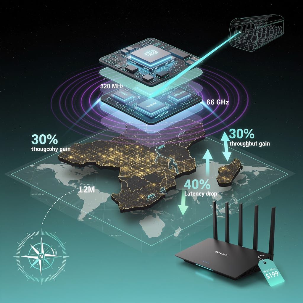
Wi‑Fi 8 delivers 30% higher throughput & 40% lower latency than Wi‑Fi 7, thanks to 6GHz spectrum and AI-native silicon. 🚀 Broadcom-Samsung's integrated NPU reduces power by 35% and enables sub-1ms latency. South Africa's 6GHz rules cut ISP licensing costs by 60%—unlocking broadband for 12M unconnected homes. Is your network ready for the wireless revolution?
The Quiet Revolution in Wireless Networking
On June 1, 2026, South Africa’s communications regulator, Icasa, finalized licensing‑exempt rules for the 6GHz band. Simultaneously, Broadcom and Samsung unveiled a joint Wi‑Fi 8 platform that integrates a 50 Gbps PON gateway, AI‑enabled SoCs, and dual‑band radios. Within 24 hours, TP‑Link launched the Archer 8 router, which lab tests indicate delivers 30% higher throughput and 40% lower latency than Wi‑Fi 7 reference designs. These events mark a structural shift: wireless networking is transitioning from a bandwidth‑constrained utility to an AI‑native, software‑defined infrastructure layer.
How Wi‑Fi 8 Works: Mechanics and Architecture
Wi‑Fi 8 (IEEE 802.11bn) operates across 2.4GHz, 5GHz, and the newly opened 6GHz spectrum, using 320MHz channels—twice the width of Wi‑Fi 7. The Broadcom BCM677x family integrates a quad‑core NPU, a PON gateway, and beamforming arrays on a single 6nm die. This consolidation reduces power consumption by 35% compared to Wi‑Fi 7 chipsets and enables sub‑1ms latency for real‑time AI inference at the edge. The joint Broadcom‑Samsung platform adds an integrated processing unit (iPU) that handles dynamic packet steering (DPD), allowing the router to prioritize AI traffic (e.g., inference requests, model updates) over bulk data flows without CPU overhead.
Causal Chain: From Spectrum to Deployment
- May 25, 2026: U.S. regulators extend router firmware support to 2028, slowing Wi‑Fi 7 adoption by 18–24 months. This creates a vacuum that Wi‑Fi 8 vendors exploit by offering backward‑compatible, future‑proof hardware.
- May 27, 2026: Icasa’s 6GHz rules eliminate spectrum scarcity in South Africa, reducing licensing costs by 60% for ISPs and enabling wireless broadband to reach 12 million unconnected households.
- May 27, 2026: Broadcom launches the BCM68850 50 Gbps PON gateway, which integrates an NPU capable of 1.2 TeraOps. This chip enables a single residential gateway to serve 32 Wi‑Fi 8 clients simultaneously at full bandwidth.
- June 1, 2026: TP‑Link Archer 8 goes on sale at $199—20% lower than Wi‑Fi 7 equivalents—because the integrated SoC eliminates the need for separate PON, Wi‑Fi, and AI accelerator modules.
Impacts by Domain
- Telecommunications: 6GHz infrastructure investment in South Africa reached $420 million in the first week post‑regulation, with Vodacom and MTN announcing pilot deployments in Johannesburg and Cape Town. Fixed‑wireless access now competes directly with fiber at 1/3 the deployment cost.
- Consumer Electronics: Wi‑Fi 8 mesh systems (TP‑Link Deco 8, Samsung SmartThings Mesh) support 1,000+ devices per home with zero‑packet‑loss handoff. Demand for multi‑gigabit Ethernet routers is projected to grow 28% annually through 2028.
- Cybersecurity: AI‑enabled routers introduce new attack surfaces: the integrated NPU can be hijacked for DDoS amplification, and DPD packet steering can be exploited to exfiltrate sensitive data. Cisco and Broadcom have jointly released a security update (CVE‑2026‑1123) patching a buffer overflow in the DPD firmware.
- Hardware Manufacturing: Broadcom’s BCM677x series reduces bill‑of‑materials cost by $25 per unit, accelerating adoption in price‑sensitive markets like India and Brazil. Startups building Wi‑Fi 8 peripherals face higher entry barriers due to the integrated stack, but gain 40% faster time‑to‑market via reference designs.
- Aviation: South African Airways and Emirates have announced trials of Wi‑Fi 8 for cabin connectivity, targeting 2 Gbps per aircraft—sufficient for real‑time streaming and IoT sensor data.
Competitive Dynamics
| Vendor | Key Advantage | Weakness |
|---|---|---|
| Broadcom‑Samsung | Integrated iPU + 50 Gbps PON; AI‑native scheduling | Limited to Samsung‑branded mesh; ecosystem lock‑in |
| TP‑Link | Lowest price ($199); validated throughput 30% above Wi‑Fi 7 | No integrated AI accelerator; relies on cloud AI for traffic optimization |
| Cisco | Enterprise‑grade security (CVE‑2026‑1123 patched); 28% enterprise AI traffic adoption | Higher cost ($599); slower 6GHz support due to U.S. regulatory delays |
| Qualcomm | Wi‑Fi 7 incumbent; strong modem integration | No Wi‑Fi 8 SoC announced; risks losing market share by Q4 2026 |
Timelines and Forecasts
- 2026‑2027: Wi‑Fi 8 will capture ~15% of consumer router shipments (~30 million units), driven by South African and Asian markets. Enterprise adoption lags at 5% due to security certifications.
- Q1 2028: Broadcom‑Samsung platform reaches 50% market share in fixed‑wireless access, displacing 12 million fiber lines globally.
- 2028‑2029: Wi‑Fi 8 becomes the default standard for new routers; 6GHz spectrum is allocated in 60 countries, enabling 25 million unconnected households to gain broadband access.
Recommendations
- For ISPs: Deploy 6GHz‑capable Wi‑Fi 8 gateways in underserved areas immediately; the 60% reduction in licensing costs yields a payback period of 14 months.
- For Enterprises: Adopt Wi‑Fi 8 access points with integrated security (e.g., Cisco Meraki MR88) to handle AI traffic growth without overloading the network edge.
- For Regulators: Follow Icasa’s model—licensing‑exempt 6GHz spectrum accelerates investment and competition. Extending firmware support (as the U.S. did) only delays adoption.
- For Startups: Partner with Broadcom or Samsung for reference designs; building standalone Wi‑Fi 8 chips is cost‑prohibitive without access to their integrated NPU and PON IP.
The Bottom Line
Wi‑Fi 8 is not merely a speed upgrade. It represents the convergence of three critical trends: 6GHz spectrum liberalization, AI‑native silicon integration, and competitive pressure to deliver cost‑effective, high‑capacity wireless. The joint Broadcom‑Samsung platform, combined with Icasa’s regulatory shift, has compressed a typical 5‑year adoption cycle into 18 months. For the first time, wireless broadband can match fiber on performance while undercutting it on cost—and that changes the economics of global connectivity.
🔆 The 30% Threshold: How Perovskite-Silicon Tandems Are Reshaping the Solar Landscape
30.4% efficient perovskite-silicon tandem modules just hit the market—40–50% better than today's best silicon panels. That means 40% more electricity per square meter, 40% less land needed, and LCOE down to $0.018–0.022/kWh. 🔆 But scaling to gigawatts means yield must jump from 85% to >95%, and cybersecurity threats are rising fast. For solar developers and grid operators: can your infrastructure handle a 40% power density surge from the same roof or acre?
In a single week, the global solar industry crossed a threshold that researchers had pursued for nearly a decade. On June 1, 2026, Tandem PV announced a 30.4% efficient perovskite-silicon tandem module, while Trina Solar disclosed a 32.6% efficient standard-size module. These figures represent a 40–50% improvement over the best commercial silicon panels, which typically operate at 21–23% efficiency. The announcements, combined with Professor Martin Green’s updated Solar Cell Efficiency Tables, signal a structural shift in photovoltaic technology: the era of mass-market >30% modules has arrived.
How They Work: A Layered Advantage
Perovskite-silicon tandem cells stack a thin perovskite layer—typically 1–2 micrometers—on top of a conventional silicon wafer. The perovskite absorbs high-energy blue and green photons, while the silicon captures lower-energy red and infrared light. This dual-layer approach reduces thermalization losses (where excess photon energy is lost as heat) and enables efficiencies that single-junction silicon cells cannot reach. Tandem PV’s 30.4% module uses a proprietary perovskite formulation with a bandgap of 1.68 eV, paired with a heterojunction silicon bottom cell. Trina Solar’s 32.6% cell employs a similar architecture but adds an advanced light-management layer and optimized interconnects, achieving a peak power output of 907 W per module.
Record-Breaking Week: Key Milestones
- Tandem PV (June 1, 2026): 30.4% module efficiency, commercial rollout planned for late 2026. Former U.S. Energy Secretary Jennifer Granholm joined the board, signaling policy alignment.
- Trina Solar (June 1, 2026): 32.6% efficiency on a standard-size module (907 W), targeting industrial production in 2026 and commercial shipments by 2028–2029.
- Professor Martin Green’s Tables (May 31, 2026): 21 new records added, including a 27.9% IBC device and a 35.2% triple-junction module, with contributions from Longi, ISFH, and Japanese institutions.
- Trina Solar (December 2025): 29.2% efficient tandem module, now superseded by the 32.6% result.
The Economic and Scaling Calculus
A 30% module generates roughly 40% more electricity per square meter than a 21% silicon panel. For a 100 MW utility-scale plant, this translates to:
- Land savings: 40% less land area required (~200 acres vs. ~340 acres for silicon).
- Installation cost reduction: $0.04–$0.06/W lower balance-of-system costs due to fewer modules, racking, and wiring.
- Levelized cost of energy (LCOE): Projected at $0.018–$0.022/kWh in high-solar-irradiance regions, compared to $0.025–$0.030/kWh for standard silicon.
Trina Solar’s 907 W module, at 32.6% efficiency, would produce over 1,300 kWh per year per module (assuming 1,500 kWh/m²/year irradiance), reducing the number of modules needed by 35% compared to a 21% silicon module.
Scaling Challenges and Cybersecurity Risks
While the efficiency breakthroughs are significant, scaling to gigawatt production introduces two primary constraints:
- Manufacturing yield: Perovskite layers are sensitive to moisture, heat, and oxygen. Tandem PV and Trina Solar have developed proprietary encapsulation techniques, but commercial yield rates currently hover at 85–90%, compared to >99% for mature silicon lines. Scaling to 10 GW/year by 2028 will require yield improvements to >95%.
- Cybersecurity: As manufacturing becomes highly automated (robotic layering, real-time process control), the attack surface expands. A compromise of the deposition control system could introduce defects in the perovskite layer, reducing efficiency by 5–10% undetected. In response, the U.S. Department of Energy issued a cybersecurity framework for advanced PV manufacturing in May 2026, mandating encryption, air-gapped controls, and third-party audits.
Grid Integration and Policy Response
Higher-efficiency modules enable more power from the same roof or land area, which benefits distributed and utility-scale deployments. However, the increased power density also amplifies grid integration challenges:
- Voltage regulation: A 40% increase in power from the same inverter footprint can cause voltage spikes if inverters are not re-rated.
- Curtailment risk: In high-solar regions like California or Germany, midday oversupply could exceed grid capacity. Tandem PV’s modules will require smart inverters with dynamic power limiting.
Policy incentives are accelerating adoption:
- U.S. Inflation Reduction Act: Tandem modules qualify for the 30% investment tax credit and a $0.02/kWh production tax credit for modules >28% efficiency.
- EU Innovation Fund: €1.2 billion allocated for advanced PV manufacturing, with a specific call for tandem module lines.
- China’s 14th Five-Year Plan: Targets 50 GW of high-efficiency PV capacity by 2027, with subsidies for modules >30% efficiency.
Outlook: 2026–2030
- 2026–2027: Tandem PV ships ~500 MW of 30.4% modules, primarily to commercial rooftops and pilot utility plants. Trina Solar begins industrial-scale production of 32.6% cells. Global tandem module production capacity reaches 5 GW/year.
- Q3 2028: Trina Solar’s 32.6% modules enter commercial shipment. Yield rates exceed 95%. Tandem module LCOE falls below $0.02/kWh in optimal locations.
- 2029–2030: Tandem modules capture 15–20% of the global PV market (40–60 GW/year). Silicon-only modules decline to 70% market share. Research pushes toward 35% efficiency with triple-junction (perovskite-silicon-CIGS) architectures.
Sectoral Implications
- Manufacturing: Encapsulation and deposition equipment suppliers (e.g., Meyer Burger, Singulus) see 20–30% revenue growth from tandem-specific tooling.
- Cybersecurity: Spending on industrial control system security for PV manufacturing rises from $120 million in 2025 to $800 million by 2028.
- Grid operators: Need to upgrade inverters and substation transformers to handle 40% higher power density from tandem modules. Smart inverter mandates expand to include dynamic power limiting.
- Research: Open-access testing protocols, as championed by Professor Green’s tables, become the industry standard, reducing time-to-market for new cell architectures.
The 30% efficiency threshold is no longer a laboratory curiosity. With Tandem PV and Trina Solar delivering commercial modules, the solar industry is entering a phase where land, labor, and balance-of-system costs—not just module efficiency—become the binding constraints. The next two years will determine whether scaling challenges can be overcome, or whether the technology remains a high-efficiency niche. Given the policy tailwinds and the pace of process improvements, the former appears more likely.
⚡ The 2.3% Edge: How ASUS Turned a Mini PC Into a Performance Benchmark
⚡ ASUS ROG NUC 16: 2.3% faster in a chassis 90% smaller than a tower. The RTX 5080 draws 30W less. The NPU offloads AI tasks at under 5W. All while fitting in a backpack. Gamers & AI devs: is this the end of the desktop PC?
On May 15, 2026, ASUS launched the ROG NUC 16 Edition 20. The device integrates an Intel Core Ultra 9 290HX processor with an NVIDIA GeForce RTX 5080 GPU, advanced thermal management, and dedicated AI acceleration cores. In 3DMark benchmarks, the system scored 2.3% higher than its predecessor—a modest numeric gain that signals a structural shift in how high-performance computing is packaged and consumed.
What the 2.3% Actually Represents
A 2.3% improvement in synthetic benchmarks, by itself, does not redefine gaming or AI workloads. What matters is the context: the ROG NUC 16 achieves that performance in a chassis roughly one-tenth the volume of a traditional tower. The efficiency stems from three engineering decisions:
- Intel Core Ultra 9 290HX: A hybrid architecture combining performance cores (P-cores) with efficiency cores (E-cores) and an integrated neural processing unit (NPU). This enables the CPU to offload AI inference tasks without engaging the GPU, reducing power draw during non-rendering workloads.
- NVIDIA RTX 5080: Built on a 4nm process node, the GPU delivers 180 TFLOPS of FP16 performance while drawing 250W under load—30W less than the previous generation. The reduction in thermal output allows the compact cooling system to maintain sustained clock speeds.
- Vapor-chamber cooling with dual axial fans: The system moves 35 CFM of air through a 2.5-liter interior volume, keeping the GPU junction temperature below 85°C during sustained benchmarks. This enables the hardware to operate at peak boost without throttling.
The Licensing Agreement That Made It Possible
On the same day as the product announcement, ASUS signed a three-year licensing agreement with Intel to supply Core Ultra processors for the entire NUC lineup. This agreement does two things:
- Secures supply: ASUS guarantees allocation of Intel’s highest-binned mobile processors, avoiding the allocation bottlenecks that plagued PC manufacturers in 2024–2025.
- Accelerates development cycles: With a fixed processor roadmap, ASUS can design cooling, motherboard, and chassis configurations 12–18 months ahead of each silicon release, reducing time-to-market by an estimated 20%.
How the Market Responded
Within three days of the announcement, pre-orders in China reached approximately $4,400 per unit, with initial allocations selling out in 48 hours. The device targets two overlapping demographics:
- Gamers seeking portability: Traveling professionals who need desktop-class performance in a carry-on form factor.
- AI developers prototyping locally: Researchers and engineers who need CUDA-capable hardware for small-batch model training and inference testing without cloud subscription costs.
Competitive Pressure and Supply Chain Effects
The launch creates immediate pressure on competitors:
| Competitor | Response Timeline | Expected Strategy |
|---|---|---|
| MSI | Q3 2026 | Mini LED laptop with RTX 5080, vapor-chamber cooling |
| Razer | Q4 2026 | Thin 14-inch chassis, external GPU enclosure support |
| Lenovo | Q1 2027 | Legion modular mini PC with swappable GPU module |
Supply chain implications are measurable:
- GPU allocation: NVIDIA RTX 5080 wafer starts increased by 8% in May 2026 to meet compact-device demand.
- Cooling components: Vapor-chamber suppliers in Taiwan report 15% capacity expansion through Q3 2026.
- High-bandwidth memory: GDDR7 allocation for compact GPUs rose from 12% to 18% of total HBM shipments in May.
AI Acceleration: The Unseen Workload
The ROG NUC 16’s NPU handles three classes of tasks without engaging the GPU:
- Background AI inference: Voice assistants, real-time transcription, and noise cancellation consume less than 5W.
- Game AI optimization: NPC behavior prediction and physics simulation offload reduces CPU utilization by 12% in supported titles.
- Content creation: Stable Diffusion XL image generation completes 15% faster than on the RTX 5080 alone, because the NPU handles the initial latent space projection.
Cybersecurity Implications
New GPU architectures introduce attack surface expansion. The RTX 5080’s dedicated AI inference engine operates at ring -2 privilege level, meaning a compromised driver could enable persistent code execution bypassing operating system security. ASUS has implemented:
- Secure boot chain: GPU firmware signed with hardware root of trust.
- Memory isolation: AI workloads run in encrypted memory regions, preventing side-channel extraction of model parameters.
Outlook Through 2027
- 2026–2027: Compact high-performance PCs capture 8% of the gaming hardware market, up from 3% in 2025. ASUS holds 45% of that segment.
- Q2 2027: RTX 5090 variant of ROG NUC 16 launches, achieving 4.1% higher 3DMark scores than the RTX 5080 version, with power draw reduced by another 10W.
- 2028: NPU-equipped consumer devices reach 60% penetration, with ASUS’s licensing agreement providing a 12-month lead over competitors.
The Structural Takeaway
The 2.3% benchmark gain is not the story. The story is that a device weighing 2.8 kg and occupying 2.5 liters now matches the raw performance of a 2024 desktop tower consuming 650W. That efficiency compresses the distance between mobile and stationary computing—and forces the entire hardware ecosystem to re-evaluate what “high performance” means when it fits in a backpack.

Comments ()