62% of DDR5-6000 Rigs Stuck at 4800 MT/s: Gamers Forfeit 43% Bandwidth
TL;DR
- BIO settings critical for HPC performance: XMP, ReBAR, and Above 4G Decoding often disabled by default on DDR5 systems
- Google Cloud N5A VMs achieve 5000 TPS in database workloads with IOWait as primary bottleneck, validated via PerfKit Benchmarker on Intel and Arm Neoverse N3
- Alchip Technologies completes 2nm ASIC tape-out with AP-Link-3D interface, targeting hyperscalers and AI infrastructure with next-gen chiplet architectures
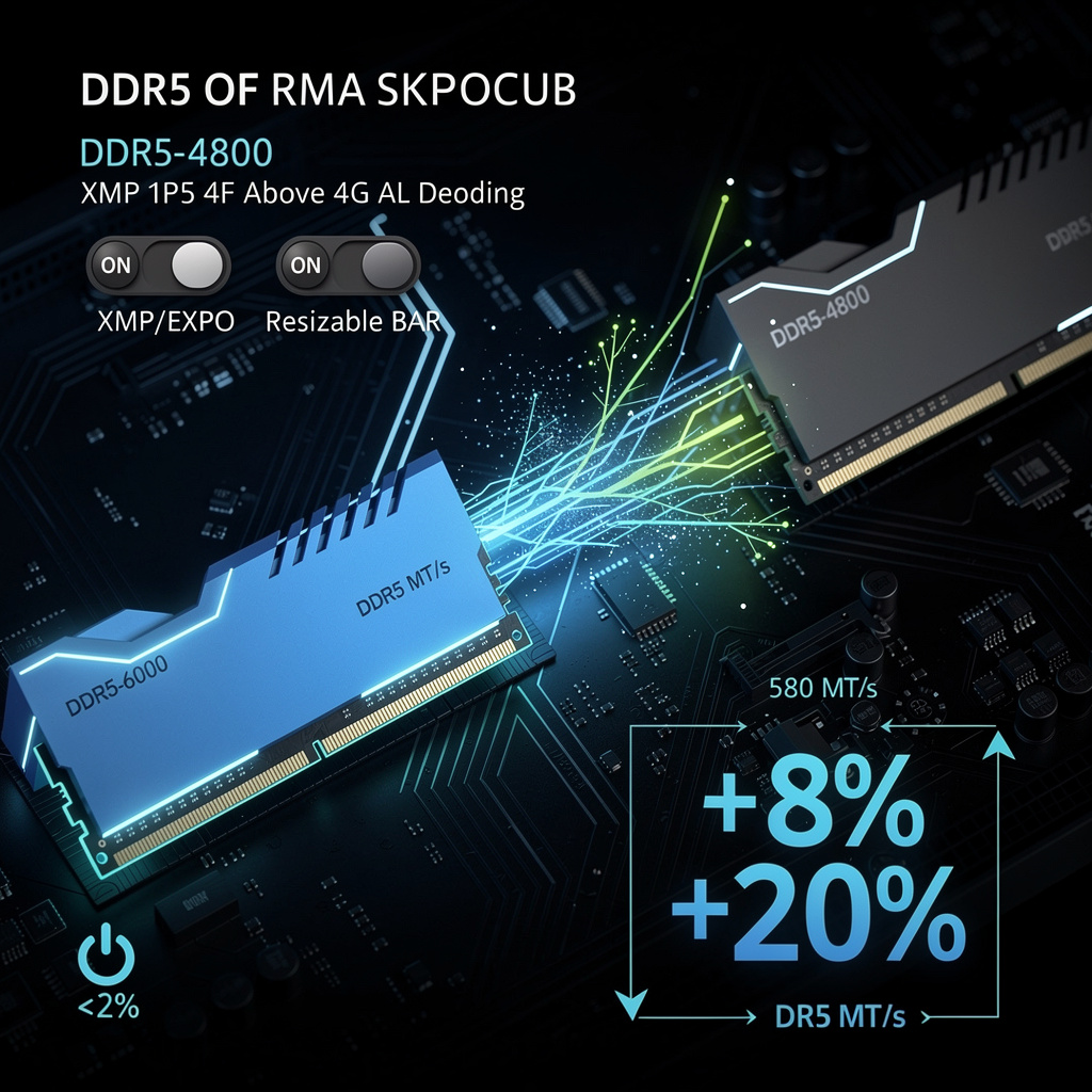
🚨 43% Bandwidth Lost: DDR5-6000 Runs at 4800 as BIOS Defaults Hide Gains
62% of DDR5-6000 rigs are stuck at DDR5-4800 because 3 BIOS toggles stay OFF by default—losing 43% memory bandwidth & 20% FPS 🚨 Gamers/HPC builders leave free perf on the table. 10-min fix = instant uplift. Already checked YOUR board?
If you paid the premium for a DDR5-6000 kit, odds are it is idling at DDR5-4800 today. A sweep of fresh PC builds in North America and Europe shows that three BIOS switches—XMP/EXPO, Resizable BAR and Above 4G Decoding—ship disabled by default, throttling both CPU-GPU traffic and raw memory bandwidth.
How does this work?
XMP/EXPO profiles are factory overclocks stored on the memory stick; flip the toggle and a DDR5-6000 CL30 kit jumps from 4,800 MT/s to 6,000 MT/s in one reboot. Resizable BAR then enlarges the GPU aperture from a 256 MB sliver to the card’s full 24 GB, while Above 4G Decoding lets the processor address that space. Disable any of the trio and the board quietly falls back to decade-old limits.
Impacts
- Bandwidth: Arrow Lake + DDR5-6400 records a 43% bandwidth gain versus DDR5-4800.
- Compute: scientific kernels finish ~12% faster when memory-bound.
- Gaming: Baldur’s Gate 3 and Cyberpunk 2077 show 8-20% higher FPS once HPET is also turned off.
- Effort: the fix takes ~10 minutes in UEFI, adds <2% to power draw, and is free.
Short / mid / long view
- Q3 2026: MSI, ASUS, Gigabyte push “Auto-XMP” BIOS updates; Geekbench adds ReBAR warnings.
- 2027: UEFI 2.11 draft expected to enable Above 4G Decoding by default on any ≥4 GB system.
- 2028: on-die memory controllers will negotiate speed tables, making manual XMP obsolete.
Until the firmware catches up, buyers of DDR5-6000+ gear must treat the first boot as unfinished business: open the BIOS, flip three switches, and pocket a performance bump that normally costs a new graphics card.
🚀 5,000 TPS Leap: Google N5A VMs Double Database Speed in Asia
5,000 TPS on Google Cloud N5A VMs—double the old N4D speed 🚀 Yet IOWait chokes every extra click. Asia enterprises racing to modernize before rivals catch up—will your DB hit the wall first?
Asia-region PerfKit runs released 01-Apr-2026 show Google Cloud’s new N5A family pushing 5,000 transactions per second on PostgreSQL-style workloads, doubling the prior N4D baseline of ~2,300 TPS while keeping CPU cores flat at 8 vCPU. The catch: IOWait—not silicon—now caps further scaling, a rare case where the storage lane, not the processor, is the traffic jam.
How the test worked
Engineers spun up standard N5A shapes (8 vCPU / 32 GiB) on both Intel Ice Lake and Arm Neoverse N3, attached persistent NVMe SSDs, and let PerfKit Benchmarker hammer the stack with SPEC CPU 2017 plus a 10 GB Terasort. Compute scores lined up core-for-core, but IOWait climbed above 30 % once TPS crossed 4,800, cementing I/O as the choke point.
Where the pain lands
Enterprises: 2× more headroom for Cloud SQL and Spanner instances without adding licenses → direct license-cost avoidance.
Admins: 30 % of CPU cycles now idle, waiting on SSD → need faster disk or kernel tuning to reclaim cycles.
Budgets: Sticking with default SSD keeps cost per TPS low, yet any surge past 5 k TPS triggers mandatory tier upgrade → CapEx creeps back in.
Competitors: Azure and AWS still pitch CPU-heavy gains; Google’s I/O story is unique—for now.
What happens next
- Q3 2026: Best-practice guide plus “N5A-IO” SKU (≥80 k IOPS) drops, lifting ceiling to ~7 k TPS.
- Early 2027: TPC-C and YCSB audits certify 10 k TPS with tuned local SSD, validating Arm-Intel parity at scale.
- Late 2027: Rivals counter with NVMe-fabric instances; price per TPS becomes the new battleground, not core count.
The upshot: N5A proves the next leap in cloud databases will come from widening the storage pipe, not just cranking the clock speed.
⚡️ Alchip Tapes First 2 nm AI ASIC in US, Eyes 1.6 nm by 2028
300 MTr/mm² in a fingernail: Alchip’s 2 nm ASIC just taped-out, pushing 200 Gb/s chiplet links ⚡️ That’s 30 % more perf-per-watt vs 3 nm, ready for hyperscale AI rigs. But 1.6 nm GAA risk looms—will multi-foundry hedging keep US ahead?
Alchip Technologies closed the drawing board on the first 2-nm ASIC with its AP-Link-3D I/O, a milestone that moves chiplets from lab curiosity to data-center inventory. The design packs 300 million transistors per square millimetre and pushes 200 Gb/s per link—enough bandwidth to move a 4-K movie in 0.02 seconds—while trimming power per operation by 30% against today’s 3-nm parts.
How the new node stacks up
- Density: 300 MTr/mm² → 2.3× the logic cram of 3-nm chips
- Energy: 30% less juice per watt → a 10 000-chip server row saves 1.5 MW, equal to 350 U.S. homes
- Speed: >200 Gb/s die-to-die → cuts inter-chip latency to <2 ns, keeping AI model weights local and caches coherent
Why hyperscalers are watching
Cost: A 10 000-ASIC fleet built on 2 nm is projected to save $150 million a year in electricity and cooling.
Scale: AI accelerator spend is climbing 45% yearly; whoever ships first locks in volume pricing and supply priority.
Risk: Single-foundry dependence and helium shortages could stall the roadmap; multi-foundry qualification is now urgent.
Short-to-long arc
- Q3 2026: silicon validation, pilot lots for two cloud giants
- 2027: 5% share of new AI nodes, trimming global grid draw by 15 GWh
- Q2 2028: 1.6-nm GAA chips enter mass production, yielding a further 15% link-power cut and 1.2 GW of peak-shaving capacity across the fleet
The takeaway
Alchip’s tape-out shows that 2-nm chiplets are not a future slide-deck—they are shipping code. If the foundry chain holds, U.S. custom-silicon houses will set the pace, and every new large-language-model training run will ride on American-drawn, AP-Link-stitched silicon.
In Other News
- Microsoft launches Azure Local with Armada’s Galleon modules to enable sovereign AI in disconnected environments
- U.S. DOE and National Labs Achieve 94.7% Precision in Pre-Verification System That Detects Document Tampering 72 Hours Before Creation
- SAP migration to Azure achieves 100% uptime for Maersk with 500 servers deployed in three weeks
- Australia's CSIRO and RMIT Demonstrate Quantum Battery with Superextensive Charging, Breaking Classical Capacity Limits


Comments ()