32 TB/s AI Bandwidth Breakthrough — NVIDIA Leads as Europe and Asia Lag Behind
TL;DR
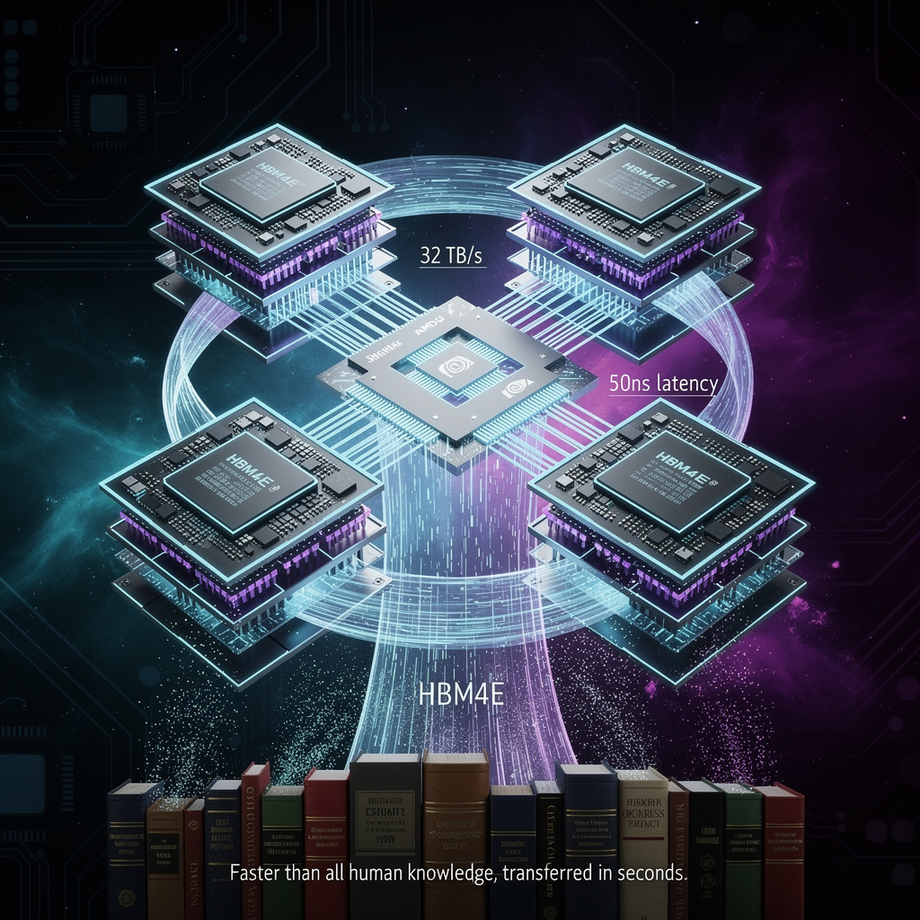
- Rambus Announces HBM4E Memory Controller IP with 32 TB/s Bandwidth for AI Accelerators
- Imec and Atlas Data Storage co-develop DNA-based storage system on 300mm CMOS platform, enabling petabyte-scale archival for HPC workloads
- Apple Unveils M5 Pro and M5 Max Chips with 4x AI Compute Boost and Fusion Architecture
🚀 32 TB/s Memory Bandwidth: Rambus HBM4E Controller Shatters AI Limits in Taiwan
32 TB/s memory bandwidth — a new ceiling for AI. 🚀 That’s 4x the bandwidth of a supercomputer rack, packed into a single GPU chip. Rambus & Samsung just unlocked it with HBM4E — but only early adopters like NVIDIA get it first. Who gets left behind when training a 175B LLM drops from weeks to days? — Data-center teams in Europe and Asia
Rambus has introduced its HBM4E memory controller IP, the fastest interface architecture yet announced for high-bandwidth memory, delivering 32 terabytes per second across eight stacked modules—enough throughput to transfer the entire printed collection of the U.S. Library of Congress in under three seconds. The announcement, made March 4, positions the company to capture early licensing revenue as NVIDIA, AMD, and data-center operators race to deploy more powerful AI accelerators.
How the architecture achieves this throughput
The controller supports 16 gigabits per second per pin, the maximum rate under current JEDEC standards, yielding 4.1 TB/s per HBM4E stack. Eight stacks operating in parallel reach the 32 TB/s aggregate figure. Latency clocks in at or below 50 nanoseconds, with 2.5-D interposer and full 3-D packaging options. Built-in error correction, on-die temperature sensors, and adaptive voltage scaling address reliability concerns that escalate with higher data rates.
What this enables—and complicates
Training efficiency: IDC analysis indicates large language model workloads are memory-bandwidth constrained; the 60% throughput increase over prior HBM4 controllers can reduce training time by roughly 30% for equivalent compute clusters.
Integration burden: Higher pin counts demand more sophisticated board-level routing, and HBM4E die supply from partner Samsung remains unproven at scale.
Competitive pressure: SK Hynix and Micron are accelerating their own HBM4/E roadmaps, while HBM5 development looms beyond 2028.
Market positioning and risks
Rambus holds a first-mover advantage through its Samsung partnership and immediate licensing availability, but this window may narrow quickly. The company's reliance on early-access customers delivering reference designs creates execution risk, and any supply-chain disruption in through-silicon-via manufacturing could stall adoption.
Adoption trajectory
- Q2 2026: Licensing program opens; design-enable kits with pre-validated interposer layouts offered to reduce OEM integration risk.
- H2 2026: First silicon integration expected in NVIDIA and AMD reference GPUs.
- Q4 2026: Commercial availability to OEMs; licensing revenue projected up 45% year-over-year.
- 2027–2028: Broad data-center deployment; Google and Microsoft pilots report 20–30% reduction in training epochs for 175-billion-parameter models.
Sectoral shift
The specification establishes a new baseline for AI accelerator memory bandwidth, likely pressuring energy-efficiency standards as data centers absorb higher-throughput hardware. Rambus's reliability extensions aim to offset power growth, but the broader test will be whether HBM4E achieves market dominance before HBM5 emerges—or whether the window for this generation proves narrower than the architecture's speed suggests.
🧬 215 PB per Gram: DNA Storage Breakthrough on Silicon Chips Reshapes US Data Archival
215 PB per gram of DNA — that’s 215 million GB — stored in a single chip the size of a coin 🧬. Imagine archiving all of YouTube’s history in a sugar cube. This isn’t sci-fi: IMEC and Atlas just built it on standard silicon wafers. But write speeds? Still hours per petabyte. Who holds the keys to the next century of data — engineers, or the regulators slowing DNA production? 🤔
IMEC and Atlas Data Storage have unveiled a DNA-based archival system that integrates millions of nanoscale electrochemical synthesis sites onto a standard 300mm CMOS wafer, achieving storage densities of hundreds of petabytes per device—roughly equivalent to archiving the entire printed collection of the Library of Congress more than 150 times over in a single chip-sized unit.
How does this work?
The system pairs IMEC's semiconductor manufacturing expertise with Atlas-designed control ASICs to enable parallel DNA synthesis across millions of independently addressable sites. Each site writes data by assembling nucleotide sequences electrochemically, with the CMOS layer providing precise voltage control. Readout relies on nanopore sensors that sequence DNA strands at approximately 3 MB/s per sensor, with multiplexed arrays scaling beyond 100 MB/s for bulk retrieval. Current prototypes demonstrate ~90% raw read accuracy, addressable through error-correcting codes to achieve archival-grade integrity.
What changes in the data landscape?
Energy: Data centers consumed roughly 1.5% of global electricity in 2024, with AI training workloads driving double-digit annual growth. DNA storage operates at negligible idle power, eliminating the cooling and continuous refresh cycles required by magnetic tape and disk arrays.
Density: A single gram of DNA theoretically stores ~215 million GB; the IMEC-Atlas device targets 200–500 PB per unit, compressing exabyte-scale archives from warehouse footprints to rack-mounted cartridges.
Cost: Synthetic DNA synthesis currently runs near $5 million per gigabyte, but wafer-scale parallelization projects a 10× cost reduction within 2–3 years, with long-term targets below $10,000 per petabyte.
Durability: Properly stored DNA remains readable for centuries to millennia, outlasting magnetic media's 10–30 year lifespan and matching glass-based alternatives without their specialized readout hardware.
Competing pathways to cold storage
DNA-based (IMEC-Atlas): Hundreds of PB per device; rewritable via emerging nanopore methods; semiconductor-compatible manufacturing.
Glass 5-D (Microsoft Project Silica): Millennial durability; ~4.8 TB per layer; write-once limitation; lower density by three orders of magnitude.
Bio-hybrid perovskites: Sub-0.1V operation; 250°F thermal tolerance; experimental stage; targets low-power memory rather than archival density.
Where development accelerates and stalls
Strengths: CMOS integration enables immediate scaling to existing 300mm fabrication lines; passive retention eliminates energy-intensive data migration every decade.
Weaknesses: Write speeds remain minutes per gigabyte; read throughput lags behind tape and optical systems; error rates demand substantial coding overhead.
Opportunities: Direct integration with cloud tiering APIs; hybrid hot-cold architectures pairing flash for active data, DNA for archival snapshots.
Threats: Regulatory scrutiny of large-scale synthetic DNA production; nucleotide supply chain constraints at production volumes; competing technologies capturing early enterprise commitments.
What comes next
- 2026–2027: Pilot wafer production and national laboratory field trials; cost reduction to ~$500,000 per gigabyte; read accuracy stabilization above 85%.
- 2028–2029: Commercial DNA-archival cartridge release at 300+ PB capacity; API standardization enabling cloud provider integration; rewritable nanopore interfaces demonstrated.
- 2030–2031: Enterprise pricing below $10,000 per petabyte; adoption across genomic research consortia and AI training pipeline archival; hybrid storage tiers reducing data center cooling loads by 40% or more for cold workloads.
The IMEC-Atlas system transforms DNA storage from laboratory curiosity to manufacturable infrastructure by anchoring it in semiconductor economics. For scientific computing and AI operations generating petabytes of training data that must persist but rarely change, the technology offers a pathway to decouple archival growth from energy consumption—provided synthesis costs continue their projected descent and read speeds approach practical thresholds for bulk retrieval.
🤯 4× AI Compute Power: Apple’s M5 Max Launches with $2,700 Price Tag and RAM Shortages — United States
4× AI compute power in a laptop? 🤯 That’s like fitting 4 MacBooks’ worth of brainpower into one. The new M5 Max delivers this — and 128GB unified memory — but costs $2,700+. Professionals gain speed; indie creators face a $200 price wall. Who gets left behind when AI tools demand this kind of hardware?
Apple has launched the M5 Pro and M5 Max processors, introducing Fusion Architecture—a dual-die design that delivers up to four times the peak AI compute of its predecessor while pushing memory bandwidth to 614 GB/s. The chips power refreshed 14-inch and 16-inch MacBook Pros available March 11, marking Apple's most aggressive silicon advancement since the M1 transition.
How Fusion Architecture Works
The design splits processing across two 3 nm dies: one dedicated to CPU functions, the other to GPU and media engines. A unified memory controller bridges both dies, preserving the single memory pool that defines Apple Silicon while doubling effective bandwidth. The CPU employs 18 cores—six high-performance "Super-cores" plus 12 efficiency cores—while GPU cores scale from 20 (M5 Pro) to 40 (M5 Max). The Neural Engine drives the 4× AI compute leap, enabling 6.9× faster large language model processing versus the M1 Pro.
Performance Gains and Trade-offs
Compute: 30% faster professional workloads; 2.5× multi-threaded throughput versus M1 generation Graphics: 35% ray-tracing improvement; 7.8× faster AI-image generation Storage: PCIe 4.0 NVMe SSDs reaching 14.5 GB/s—double prior speeds Connectivity: Thunderbolt 5 (80 Gb/s) and Wi-Fi 7 standard
Cost: $200 base price increase; 128 GB RAM configurations add $1,200 Supply: High-capacity unified memory strains DRAM availability Clarity: Conflicting reports on Neural Engine cores (16 versus 32) risk consumer confusion
Competitive Positioning
Apple claims 20–40% graphics performance leads over AMD Ryzen 7000 mobile and Intel Xe-HPG alternatives, with 30–40% advantages in AI compute. The integrated Media Engine accelerates ProRes and machine-learning pipelines, reinforcing vertical integration against Windows workstations that typically require discrete components for comparable throughput.
What Comes Next
- March–August 2026: Benchmark validation (Geekbench 6, MLPerf); early adoption by film studios and AR/VR developers; potential 128 GB RAM supply constraints
- 2027–2028: Fusion Architecture likely extends to Mac Studio and Mac Pro; third-party AI frameworks increasingly optimize for Metal and Neural Engine; competitors accelerate 3 nm roadmaps to close the AI-compute gap
The M5 generation positions Apple to capture on-device inference workloads—processing that previously required cloud infrastructure—while compelling rivals into costly silicon transitions. Success hinges on resolving memory supply constraints and eliminating specification ambiguity that could slow enterprise adoption.
Four times the AI compute translates to practical capabilities: a 10-billion-parameter language model now runs locally in roughly the time an M1 Pro handled 1.5 billion parameters, or real-time 8K video stabilization that previously demanded render farms. These are not marginal gains but threshold shifts that redefine what portable hardware accomplishes.
In Other News
- Pico Unveils Pico OS 6 and Project Swan for Productivity-Focused XR Headsets in 2026
- TECNO unveils Edge-Side AIGC Preview at MWC 2026, enabling 30fps on-device generative AI rendering via Armv9 and KleidiAI on 1600+ global markets
- Apple unveils MacBook Neo with A18 Pro chip, starting at $599, featuring 16-hour battery life and 3x faster AI workloads
- Huawei and China Unicom collaborate on AI-centric all-optical network infrastructure at MWC Barcelona 2026, targeting 50ms latency


Comments ()