1,000W EUV Breakthrough: 50% Faster Chip Output Fuels Exascale Race—But Monopoly Risks Loom
TL;DR
- ASML Breaks Through EUV Power Limits to Boost Chip Output by 50% by 2030
- Microsoft's Copilot+ PCs require 40+ TOPS NPU and 16GB RAM to unlock on-device AI features like Recall, Generative Erase, and Cocreator
- Taara Photonics unveils photonic core technology delivering 25 Gbps connectivity over 10 km, deployed by T-Mobile, SoftBank, and Airtel
🔥 ASML Hits 1,000W EUV Power: 50% Chip Output Surge by 2030 Reshapes Global HPC Supply Chain
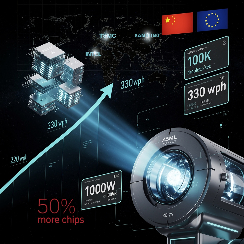
ASML just cracked 1,000W EUV power—330 wafers/hour, up from 220. That's 50% more chips per hour from the same machine. 🔥 Pilot units drop late 2026; full fleet by 2028-2030. While fabs burn 10% more power per scanner, die costs for AI GPUs could drop 10-15%—finally easing the chokehold on exascale builds. Intel gets first High-NA dibs; TSMC's $56B plan already locked in. But here's the catch: 90% market control, single-source optics, and China locked out. Is your region building the resilience to handle a 45% fab throughput surge—or still importing dependency?
ASML and Carl Zeiss AG have pushed EUV lithography past a long-standing ceiling. Their new light-source architecture, announced February 23, raises plasma-source power from 600W to over 1,000W while maintaining the 13.5nm wavelength. The result: 330 silicon wafers per hour, up from 220, with pilot machines arriving late 2026 and full deployment across High-NA scanners by 2028–2030.
How does this translate to chip production?
The physics are precise. Tin-droplet generators now fire 100,000 drops per second, feeding higher photon flux through Zeiss-fabricated optics. This throughput gain—roughly equivalent to adding another major fab's worth of capacity without new construction—enables 50% more chips per wafer by decade's end. For context, a single modern EUV scanner at this pace could process more wafers annually than the entire global output of 300mm fabs in 2010.
What changes for HPC and downstream sectors?
Cost structure: 50% higher throughput reduces per-chip mask and fab costs, lowering barriers for wafer-scale designs and dense interconnects.
Supply scalability: Accelerated EUV capacity addresses the current bottleneck constraining AI-driven HPC expansion; projected global fab capacity rises ~20% annually through 2030.
Node advancement: Sub-10nm scaling tightens pitch tolerances for GPU/CPU/TPU accelerators in exascale systems.
Energy: ~10% electricity demand increase per scanner is partially offset by efficiency-focused laser designs.
Where do risks concentrate?
Supply chain: Single-source optics and tin-droplet generators expose ASML to lead-time spikes.
Geopolitics: U.S./Netherlands export controls already pushed China's share of ASML sales from 41% to 33%; further restrictions could accelerate indigenous Chinese EUV programs.
Capital sensitivity: $50–$400 million per scanner demands flexible financing models during macroeconomic uncertainty.
Timeline and projections
- 2026–2027: 1,000W sources reach ≥30% of annual shipments; EUV bookings grow 25% year-over-year; 10–15% reduction in accelerator die costs enables earlier AI-optimized GPU deployment in exascale systems.
- 2028–2030: Full 1,000W fleet achieves ≥330 wph across all High-NA scanners; global fab throughput rises ~45%, adding roughly 2 million additional chips annually for AI/ML workloads.
ASML's FY 2025 net sales of €32.7 billion and Q4 bookings of €13.2 billion—double analyst expectations—demonstrate fabs' urgency to secure capacity. With ~90% of the global EUV market and customers including TSMC, Intel, and Samsung accounting for two-thirds of logic-fab sales, this breakthrough doesn't merely improve a machine. It reshapes the throughput ceiling for an entire technological era, positioning Europe as the critical enabler of next-generation HPC hardware while export controls and supply-chain resilience remain the variables that will determine whether the 50% output target holds.
🔒 Microsoft's 40-TOPS Gate: New Hardware Floor Locks AI Features Behind Premium Silicon
40 TOPS + 16 GB RAM = your laptop becomes an AI vault. Microsoft's Copilot+ threshold unlocks Recall, Generative Erase & Cocreator locally—200ms vs 1-2s cloud lag 🔒 But here's the catch: that 2B-parameter model eats 8-12 GB RAM, leaving crumbs for actual work. Premium devices get privacy; budget buyers get Azure dependency. Is your next laptop a gatekept AI machine or cloud-rented compute? — Which matters more: owning your AI or affording it?
Microsoft’s Copilot+ tier establishes a hard floor for on-device AI: 40 TOPS of NPU performance and 16GB of RAM. Below this threshold, features like Recall, Generative Erase, and Cocreator default to cloud execution—trading latency for accessibility.
How the hardware unlocks local AI
The 40 TOPS specification enables real-time inference without GPU assistance. Recall encrypts and indexes screen snapshots locally, answering natural-language queries in 200–400 milliseconds—roughly one-third the time of Azure fallback. Generative Erase performs in-painting directly on captured images. Cocreator runs 2-billion-parameter diffusion models to transform sketches into finished images. These workloads demand 8–12GB of RAM for model residency, leaving the 16GB baseline with narrow headroom for multitasking.
Performance trade-offs at the threshold
Latency: Local execution completes 50–70% faster than cloud routing for Recall queries.
Memory: Cocreator’s 2B-parameter model consumes 8–12GB; concurrent heavy workloads risk paging.
Storage: Recall reserves approximately 5% of primary drive capacity—about 13GB on a 256GB SSD—for encrypted snapshot buffers.
Power: Sustained NPU activity raises combined CPU-NPU thermal design power by 5–7 watts, reducing battery life roughly 10% under continuous AI use.
Vendor alignment and gaps
Qualcomm’s Snapdragon X Elite and Intel’s Lunar Lake both claim 40+ TOPS, though real-world throughput varies with quantization and driver maturity. AMD’s Ryzen prototypes and Nvidia’s workstation add-ons round out early 2026 offerings. Microsoft’s certification program aims to reduce fragmentation, but thermal throttling and inconsistent latency remain unaddressed without dynamic frequency scaling or liquid cooling in high-performance configurations.
Where capability expands or contracts
- 2026 Q1–Q2: First certified laptops ship; benchmarked Recall response improves 30–35% over cloud baseline.
- 2026 Q3: "Recall Lite" extends to 25-TOPS devices, broadening mid-tier access.
- 2027–2028: 4–8 billion parameter models push practical requirements toward 70 TOPS, likely triggering a Copilot+ threshold revision in Windows 12.
Sectoral implication
Microsoft’s specification creates a two-tier ecosystem: premium hardware retains data locally with measurable privacy and speed advantages, while legacy devices remain cloud-dependent. This bifurcation preserves market coverage across price segments but concentrates advanced AI capabilities in higher-margin silicon—accelerating replacement cycles and reshaping OEM product stacks around NPU-centric designs rather than traditional CPU-GPU metrics.
🌐 25 Gbps Airborne: Taara Beam Ditches Fiber for 10‑km Silicon‑Photon Links Across 20 Nations
25 Gbps over thin air—no fiber, no trenching. Taara Beam hits sub‑100 µs latency across 10 km with 99.999% uptime, all from a 90‑W box lighter than a carry‑on. That's fiber‑class speed deployed in days, not months. But if fog kills the link, carriers still need that hit‑less failover. Which matters more where you live: cutting install time or weather‑proof reliability? 🌐
Taara Photonics has deployed integrated-photonic backhaul systems delivering 25 Gbps over 10 kilometers without fiber, signaling a shift in how carriers bridge infrastructure gaps. The technology—now live in over 20 countries with T-Mobile US, SoftBank, and Bharti Airtel—eliminates trenching costs and months-long deployment cycles, replacing them with pole-mounted units that align in hours.
How the hardware functions
Taara Beam and Lightbridge Pro use silicon photonic integrated circuits to modulate near-infrared light into free-space optical beams. Electronic signals convert to photons at the transmitter; precision steering maintains alignment across the link. The Beam achieves 25 Gbps full-duplex; Lightbridge Pro reaches 20 Gbps with integrated hit-less failover to fiber or radio paths. Both operate below 100 µs latency and 90 watts—roughly the draw of a standard laptop—enabling direct DC power from existing cell-site infrastructure. The Beam's 8-kilogram form factor, about half the weight of a typical microwave transceiver, eliminates bulk-optic assemblies and their associated mechanical failure points.
Operational impacts
- Deployment velocity: Fiber-class capacity without civil works reduces provisioning from months to days.
- Latency positioning: Sub-100 µs round-trip supports 5G front-haul synchronization and real-time edge computing.
- Reliability architecture: Built-in optical switching preserves five-nines uptime through automatic path redundancy.
- Power economics: 90-watt consumption avoids cooling overhead required by dense radio units, lowering operational expenditure.
Carrier adoption and remaining gaps
Major deployments span the United States, Japan, India, the Caribbean, and Southern Africa. The technology originated at Alphabet's X lab, with Google providing strategic backing that lends credibility but also ties trajectory to corporate priorities. Regulatory alignment with ITU-R atmospheric models remains incomplete in several markets, and performance under heavy precipitation—rain fade at 1550 nm—requires adaptive optics refinement. Competition from 130 GHz millimeter-wave systems, which have demonstrated 120 Gbps in research settings, pressures Taara to advance wavefront steering without sacrificing cost parity.
Timeline and scaling projections
- 2026: Expanded pilots in urban corridors and rural underserved zones; interoperability demonstrations with 5G NR base stations at Mobile World Congress.
- 2027–2028: Regulatory clearance in 10+ additional markets; integration with edge AI workloads including autonomous vehicle telemetry and smart-grid monitoring.
- 2029–2030: Potential adoption for exascale data-center rack-to-rack interconnects where fiber routing proves impractical; atmospheric mitigation advances to match fiber reliability statistics.
The silicon-photonics market projects growth from $13 billion (2020) to $25 billion by 2030. Taara's positioning within this expansion depends on sustaining carrier-grade reliability while closing the bandwidth gap with emerging millimeter-wave alternatives. Success would validate free-space optics as a standard backhaul tier—failure to mitigate weather vulnerabilities risks relegation to niche, fair-weather deployments.
In Other News
- Ultima Genomics launches UG 200 series with $850K price point and 60,000 whole-genome annual throughput

Comments ()