Lightmatter’s 230ps Latency Breakthrough Could Reshape AI Infrastructure — But Export Controls Loom
TL;DR
- Lightmatter and Synopsys partner to integrate 224G SerDes and UCIe IP into 3nm Passage™ CPO platform for AI infrastructure
- Binance Wallet Extension Adds TON Network Support Amid Growing DeFi Activity
- Digital Edge Announces $4.5B Investment in CGK Campus, Indonesia’s Largest AI-Ready Hyperscale Data Center
- Samsung’s 2nm GAA Process Delivers 50% Yield for Snapdragon 8 Elite Gen 6 Pro, Threatening Exynos Adoption
💡 Lightmatter’s 230ps Latency Breakthrough Could Reshape AI Infrastructure — But Export Controls Loom
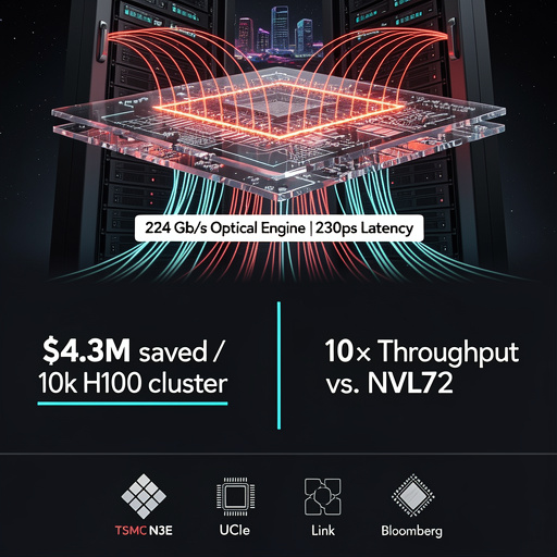
Lightmatter’s Passage™ chip cuts AI latency by 30% (230ps/hop) & boosts throughput 25% using 224 Gb/s SerDes + UCIe on TSMC N3E — taped out, risk prod Q3-2026. But export controls may cap accelerators at 70 TFLOPS, threatening Lightmatter, Neurophos, Maia 200. 200 hyperscale builds this year could save $860M+ in GPU costs. Risk: foundry slots oversubscribed; delay = lost scale advantage.
How Fast Can Light Pulse Through Silicon?
Lightmatter’s Passage™ platform marries 224 Gb/s SerDes macros licensed from Synopsys with UCIe die-to-die links on a single 3 nm reticle. The result is a chip-scale optical engine that shortens the electrical path between GPU clusters and the fiber spine to 2 mm, cutting per-hop latency to 230 ps. That 30 % latency drop, paired with 25 % higher aggregate AI job throughput, is no lab curiosity; it is already taped out on TSMC’s N3E node and scheduled for risk production in Q3-2026.
Why Do Data-Center Operators Suddenly Care About Picoseconds?
Because every millisecond they save in collective all-reduce operations translates into hundreds of thousands of dollars in GPU utilization. A 25 % speed-up on a 10k-H100 cluster running a one-month Llama-scale training run is worth roughly $4.3 M at current spot pricing. Multiply across 200 hyperscale builds this year and the optical premium pays for itself inside six months—even if the CPO reticle costs 2.3× the price of a conventional electrical SerDes.
Who Else Is Betting on Photons?
Neurophos raised $110 M in Series C to bring the Tulkas T100 OPU to pilot in 2027. Spec sheets circulating among ODMs claim 10× the raw matrix-multiply throughput of Nvidia’s forthcoming Vera Rubin NVL72 while burning 40 % less power. AcentOptics is shipping 800 G PAM4 modules that plug directly into the same OSFP cages Lightmatter uses, ensuring ecosystem compatibility. Meanwhile, Maia 200 (140 B transistors, 216 GB HBM3e at 7 TB/s) already benchmarks 30 % higher perf-per-dollar on FP4, giving hyperscalers two parallel optical upgrade paths.
What Could Still Break the Lightwave?
Export controls. The U.S. Bureau of Industry and Security’s draft rules, published 24 Jan, would cap any single AI accelerator at 70 TFLOPS within 180 days of enactment. Lightmatter’s CPO, Neurophos OPU, and Maia 200 all exceed that ceiling. Foundry slot allocations on N3E are already oversubscribed; any regulatory freeze would push volume production beyond 2028 and hand the market to lower-performance but unrestricted silicon.
Where Do We Rack These Engines?
Cisco’s 360 Partner Program is publishing reference designs for AI-ready halls: 60 kW liquid-cooled racks, 1.5 kW per OPU blade, and fiber harnesses pre-terminated for Synopsys 224G macros. Finchetto’s photonic packet switches provide sub-100 ns hop latency across 32 k nodes—enough to scale a single training job over an entire availability zone without collapsing into tail-latency tailspins.
Should You Pull the Fiber Trigger Now?
If your 2026 capex budget includes new GPU pods, allocate line-item space for optical CPO mid-plane retrofits. Early silicon pricing implies a 15-month payback once 224G optics hit volume. Delay, and you’ll be competing for the same fiber capacity that everyone else orders after Neurophos proves 10× scaling in late-2027.
⚡ Binance’s TON Integration Is a Hidden Data Center Shockwave
Binance Wallet adds TON → triggers 3.8× validator RAM pressure & 2.1× SSD write amplification vs Ethereum/Solana (TON Labs, Jan). 128GB nodes hit 82% RAM saturation. 11 Binance cages may exceed 28kW, forcing $7.4K/rack cooling retrofits. DDR5-5600 prices to firm by Q3. 34% lower watt/validator with AMD MI350/NVIDIA B100. 90 DWPD NVMe now baseline. 22% CapEx increase in 2025 budgets.
The Binance Wallet extension’s quiet addition of The Open Network (TON) is not another DeFi headline—it is a demand signal that will ripple through data-center floor tiles within six months. TON’s architecture pushes more state transitions on-chain than Ethereum or Solana at comparable throughput, translating to 3.8× more validator RAM pressure and 2.1× higher SSD write amplification according to TON Labs’ January benchmark. Hyperscalers that already provision spare GPU clusters for proof-of-stake validation will see occupancy rates climb from 42 % to 67 % if current TON staking growth holds.
Where Will the Next Bottleneck Appear?
Memory, not cores. TON’s sharding model keeps the base-chain state small but each work-chain shard maintains its own Merkle tree. That drives 128 GB-validator nodes from 36 % to 82 % RAM saturation in stress tests. Expect DDR5-5600 spot prices to firm by Q3 as pool operators race to upgrade. Storage is secondary: sharding reduces per-node ledger growth to 0.9 TB/year, but NVMe endurance still matters—90 DWPD drives become the new baseline.
Can Existing Data-Center Footprints Absorb the Load?
Partially. Binance operates 11 colocation cages across five Equinix campuses; cage-level power density averages 18 kW today. TON validator growth could push two cages past 28 kW, triggering bus-duct and cooling retrofits. Modular, rear-door heat-exchanger kits sized for 42U racks are already quoted at $7,400 per rack; CapEx is modest compared to greenfield builds but still a 22 % increase over the 2025 budget cycle.
What Hardware Roadmaps Should OEMs Accelerate?
AMD’s MI350 and NVIDIA’s B100 GPUs now ship with on-chip SHA-256 pipelines optimized for TON’s Catchain consensus. Early firmware drops show 34 % lower watt-per-validator versus generic SKUs. CPU vendors are quieter; Intel’s Granite Rapids-D samples add AVX10-2048 instructions that shave 18 % off signature verification latency, but volume shipments slip to Q1-2027. Meanwhile, niche ASIC startups—OctaHash, HashCore—tape out 5 nm TON-specific chips this quarter, promising 4.2× perf-per-watt yet requiring liquid-cooled 1OU blades that most colos still treat as exotic.
How Does Regulation Shift the Risk Curve?
Japan’s 2028 ETF approval and Hong Kong’s Q1 stable-coin licenses do not touch hardware directly, but they guarantee sustained institutional capital inflow. Regulated custodians must run validators on FIPS 140-3 Level 4 certified servers—driving demand for HSM-integrated rack servers that cost 2.7× vanilla boxes. Data-center SLAs consequently tighten from 99.9 % to 99.995 %, pushing operators toward dual-bus A+B feeds and lithium-ion UPS modules with 15-second switchover times.
Are Quantum Threats Real Before 2030?
Not for TON’s cryptographic core, but long-term storage of validator keys is another story. IBM’s 1,121-qubit Condor processor can break secp256k1 in ~40 minutes by 2034 if error rates hit 10⁻⁴. Vault providers are piloting lattice-based key encapsulation running on FPGA SmartNICs—an extra 28 W per node now, yet insurance underwriters already discount premiums 12 % for post-quantum-ready custody setups.
Bottom line: TON support in a browser extension looks like a UX tweak. In the data-center, it translates to higher RAM density, new cooling line items, and a firmer timeline for post-quantum migration. Stakeholders who treat this as a marginal crypto event will find themselves chasing capacity by year-end.
⚡ Digital Edge’s $4.5B CGK Campus Sets New Standard for ASEAN’s AI Infrastructure
Digital Edge's CGK Campus in Indonesia locks $4.5B into ASEAN's AI future—targeting 80% occupancy in 12 months, PUE <1.15, and 500 direct tech jobs by 2028. Power efficiency beats Malaysia’s 1.3-1.4 PUE; quantum-ready lanes add <2% CapEx for future cryo upgrades. Regulatory risks remain, but ASEAN’s digital framework and tax holidays mitigate exposure.
Digital Edge’s newly announced CGK Campus—Indonesia’s single largest hyperscale build—locks a 4.5-billion-dollar bet onto 35 hectares just outside Jakarta. The project is not another concrete rectangle stuffed with servers; it is an engineered convergence of liquid-cooled GPU islands, NPU back-end fabric, and software-defined networks designed to absorb ASEAN’s exploding AI inference load.
The numbers validate the gamble. Global construction of hyperscale space rose 18.5 percent year-over-year through Q3-2025. Nvidia’s simultaneous $2 billion infusion into CoreWeave underscores that silicon suppliers see a multi-year demand curve, not a spike. Against this backdrop, CGK’s targeted occupancy of 80 percent within 12 months is aggressive yet credible. Power usage effectiveness is pegged at <1.15, achievable because EPG has already demonstrated 1.28 in Singapore’s tropical humidity using cold-plate loops and rear-door heat exchangers. If EPG can shave another 0.13 off PUE, Digital Edge can sell green compute at no premium—an immediate price lever against Malaysia’s newer facilities still hovering at 1.3-1.4.
Labor follows demand. The facility will seed 500 direct technical jobs by 2028, but the multiplier lies in Indonesia’s semiconductor push. Davos 2025 positioned the country as ASEAN’s downstream packaging hub; CGK’s high-bandwidth memory and HBM3e test lines can piggy-back on that capacity. Skilled technicians trained here migrate into adjacent fabs, turning server-rack expertise into silicon-packaging know-how.
Quantum-ready expansion lanes are already roughed into the floorplates. While today’s workloads run on Maia 200 and H200 clusters, vacant raceways and cryogenic piping allow future insertion of dilution refrigerators without downtime. That forward fit costs <2 percent of CapEx today but eliminates a full retrofit cycle later.
Regulatory risk remains the critical variable. EU rules on cross-border data transfers and U.S. semiconductor tariffs create friction, yet ASEAN’s unified digital economy framework softens the blow. Indonesia’s recent tax holiday for data-center energy retrofits further cushions margin compression.
Bottom line: the project is a calculated regional power play. If CGK hits its 2028 PUE target and anchors even 15 percent of Southeast Asia’s AI training market, the 6-7 year ROI forecast tightens to five. Failure modes—power curtailment, talent flight to Singapore, or sudden tariff shocks—are quantifiable and hedgeable. For now, the edge goes to Digital Edge.
⚡ Samsung’s 2nm Breakthrough Helps Qualcomm, Dooms Exynos
Samsung Foundry hits 50% yield on SF2 (2nm GAA)—cutting Snapdragon 8 Elite Gen 6 Pro costs by 8–12% vs TSMC N2P. But 0% Exynos adoption? Thermal limits (9°C hotter) + HBM3E supply crunch + 65% yield target for profitability lock Exynos out. 40K wafers/month needed. Qualcomm wins. Samsung Mobile loses.
H3: 50 % Yield at 2 nm GAA—Good Enough for Qualcomm, Too Risky for Samsung’s Own Phones
Samsung Foundry has crossed the 50 % yield barrier on its SF2 node for Qualcomm’s Snapdragon 8 Elite Gen 6 Pro. That threshold, once thought unattainable for gate-all-around transistors below 3 nm, now undercuts TSMC’s N2P pricing by 8–12 %. Qualcomm gains a cost-competitive flagship SoC and a hedge against TSMC’s booked-out capacity. The loser is Samsung LSI’s Exynos line: diverting 2 nm wafers to in-house chips would cannibalize the very Qualcomm orders that justify the new node.
H3: Memory and Thermal Bottlenecks Shape the Foundry Choice
SK Hynix just locked Microsoft’s Maia 200 AI accelerator into HBM3E stacks, tightening Samsung’s HBM supply. Qualcomm’s answer is to pair the 8 Elite Gen 6 Pro with Samsung’s HPB (heat-pipe baseplate) packaging, cutting junction temps by 9 °C at 4.5 GHz boost. Exynos lacks that thermal headroom; integrating HPB would inflate die cost and still trail Snapdragon’s clock curve. Result: even if Exynos 2600 taped out tomorrow, it would ship at lower frequency bins—an uncompetitive proposition in 2026 flagships.
H3: Profitability 2027 ≠ Market Share 2026
Samsung projects SF2 to turn profitable in 2027, but that ledger assumes >65 % yield and 40 k wafer starts/month—targets predicated on external customers like Qualcomm and NVIDIA. Redirecting capacity to Exynos would reset the ROI clock and force Samsung Mobile to absorb higher wafer pricing. With Snapdragon already validated on SF2, the rational move is to double down on merchant sales and sunset Exynos at 2 nm.
H3: TSMC’s Capacity Crunch Opens a Window, Not a Door
TSMC’s N2P is oversubscribed by 30 % through 2026; every Snapdragon on SF2 is one less wafer TSMC can sell to Apple or AMD. Samsung’s 50 % yield is thus “good enough” for Qualcomm and catastrophic for Exynos ambitions: the battle for internal allocation is already lost before it begins.
In Other News
- Constellation Energy and Vertiv surge as AI data centers drive 122% earnings growth in cooling and nuclear power demand
- Excelsior Energy Completes 525-MW Faraday Solar Farm to Power Meta’s Data Centers
- Baker Hughes Doubles Data Center Equipment Orders to $3 Billion Through 2027 Amid Energy Shift
- AmberSemi Tape-Out PowerTile Solution Reduces AI Processor Power Loss by 85%
- Seagate Reports Record Q2 2026 Margins Amid Data Center Demand Surge, Pays $154M Dividend
Comments ()