Uink, TSMC, Blue Origin, Tezos, Neurophos Unveil Breakthroughs in Low-Power Displays, Wafer Recycling, Satellite Speed, Blockchain Efficiency, and AI Chips
TL;DR
- Uink Unveils Ultra-Efficient LoRa® e-Paper Displays with 99% Lower Power Use and 60-Month Battery Life for Global Digital Signage
- TSMC Launches Sustainability Initiative to Recycle Wafer Scrap into Dummy Dies, Saving NT$700M Annually in Advanced Packaging
- TeraWave Satellite Constellation by Blue Origin Targets 6,000x Faster Speeds Than Starlink with 6 Tbps MEO Backhaul and Enterprise-Only Access
- Neurophos unveils 470 petaFLOPS OPU chip with 10x NVIDIA Rubin performance, targeting mid-2026 production in Austin, Texas
🔋 Uink’s 5-Year Battery e-Paper Signs Set to Redefine Low-Power Digital Signage
Uink launches LoRa® e-Paper displays with 99% lower power use and 5-year battery life—set to transform digital signage in smart cities and industrial IoT by late 2026.
Uink’s new LoRa®-enabled e-Paper displays consume 99% less power than conventional digital signage, with a 60-month battery life under standard operating conditions. This efficiency leap relies on LoRa®'s low-power wide-area network (LPWAN) modulation, enabling wireless updates across kilometers with minimal energy draw.
How does this compare to current display technologies?
Typical e-Paper signage operates 12–24 months on battery, requiring frequent maintenance. Uink’s 60-month runtime reduces service frequency by up to 75%, critical for remote or hard-to-access locations. Power reduction is achieved through optimized electrophoretic materials and asynchronous LoRa® communication, which transmits only when content changes.
What infrastructure benefits emerge at scale?
Cities deploying thousands of signs can cut energy use by nearly 99% per unit. Industrial IoT applications—such as warehouse status boards or outdoor asset tags—gain reliable, long-duration visibility without grid dependency. The technology supports decentralized network topologies, aligning with open digital ecosystem standards in the EU and other regulated markets.
What limits adoption potential?
Dependence on LoRa®-compatible infrastructure creates interoperability constraints in regions using competing LPWAN standards like NB-IoT or Sigfox. Supply chain exposure to specialized LoRa® chipsets may delay scaling. Additionally, update latency—due to asynchronous transmission—limits use in high-refresh scenarios.
Where is deployment most likely by 2026?
Smart city initiatives in Europe and Southeast Asia are primary adoption targets, particularly for traffic guidance, public transit updates, and environmental signage. Retail and logistics sectors are evaluating pilot programs for inventory labeling and dynamic pricing. Uink’s partnership with LoRa Alliance members will determine rollout speed in Q3–Q4 2026.
♻️ TSMC Turns Wafer Waste into NT$700M Savings with Dummy Die Recycling
TSMC recycles wafer scrap into dummy dies, saving NT$700M yearly. The move cuts costs, reduces waste, and strengthens its lead in advanced packaging amid AI demand and geopolitical shifts.
TSMC’s new initiative repurposes wafer scrap into dummy dies, targeting NT$700 million in annual savings. The process leverages existing fabrication infrastructure to recondition silicon waste, eliminating raw material procurement and disposal costs while supporting advanced packaging for multi-chip modules.
How does this align with AI-driven demand and market dynamics?
AI infrastructure growth is intensifying demand for high-performance computing components. With NVIDIA and AMD deepening reliance on TSMC, the company’s $52–56 billion 2026 capex includes sustainability-driven innovations. Micron’s $100 billion DRAM fab in New York signals competitive pressure, while the advanced packaging services (APS) market is projected to reach $80 billion by 2033.
What are the environmental and regulatory benefits?
Direct silicon reuse reduces landfill contributions and carbon emissions from extraction. The initiative supports compliance with EU Corporate Sustainability Reporting Directive (CSRD) requirements, mitigating regulatory risk. U.S.-Taiwan tariff reductions and CHIPS Act 2.0 funding further enable circular manufacturing, particularly at TSMC’s Arizona facilities.
What technical and geopolitical risks remain?
Reprocessing must meet strict dummy die specifications, posing potential yield or quality control challenges. Intellectual property concerns may arise in overseas deployments. Despite stock gains (9% YTD) and 40.7% YoY net income growth, China’s stated 2027 target for Taiwan control introduces supply chain uncertainty.
Will competitors adopt similar models?
SK Hynix, Samsung, and Micron face rising silicon costs and regulatory pressure, making recycling economically attractive. AI-driven process mining could improve scrap sorting yields by ~20%. If validated, TSMC’s model may set a new standard for resource efficiency in semiconductor manufacturing.
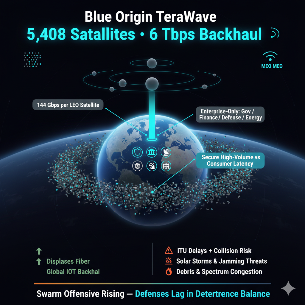
🛰️ Blue Origin's TeraWave: 6 Tbps Satellite Backhaul for Enterprises Only
Blue Origin's TeraWave targets 6,000x faster speeds than Starlink with 6 Tbps MEO backhaul—exclusively for enterprises in defense, finance, and energy. No retail access. Deployment faces regulatory, orbital, and security hurdles.
Blue Origin’s TeraWave leverages a hybrid LEO-MEO architecture with 5,408 satellites: 5,280 in low Earth orbit (520–540 km) and 128 in medium Earth orbit (8,000–24,200 km). The system delivers 6 Tbps of aggregate backhaul via 144 Gbps per-satellite throughput in LEO and 7 Tbps optical inter-satellite links in MEO. This design enables bulk data transfer at speeds exceeding Starlink’s ~1 Gbps per-user capacity by optimizing for enterprise-scale bandwidth, not consumer latency.
Why Target Enterprises Instead of Consumers?
TeraWave restricts access to governments, financial institutions, defense, and energy sectors—bypassing retail markets. This model prioritizes secure, high-volume data transport over low-latency applications. By focusing on institutional clients, Blue Origin avoids direct competition with Starlink’s 9.5 million+ users and Amazon Leo’s consumer expansion, instead displacing terrestrial fiber in secure backhaul and global IoT deployments.
What Are the Risks to Deployment?
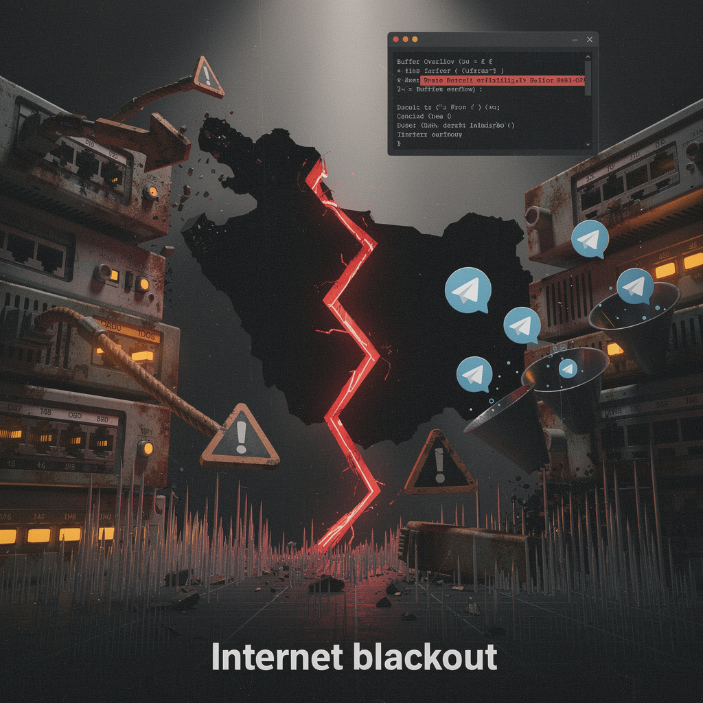
Regulatory delays loom due to ITU backlog, exacerbated by China’s 200,000-satellite filings and Rwanda’s 327,000-satellite proposal. Collision risk is high—CRASH Clock estimates a 5.5-day mean time between conjunctions. Solar storms, like the Jan 18 X1.9 flare, disrupt MEO/LEO operations. Additionally, Russia’s Tobol jamming and China’s laser targeting of satellites introduce security threats requiring hardened architectures.
Can TeraWave Scale Amid Orbital Congestion?
Scaling depends on debris mitigation and spectrum access. Atomic-6’s Space Armor tiles and precision beam alignment (0.1-degree error = 14 km displacement at 8,100 km) are critical. With private space investment up 48% to $12.4 billion in 2025, funding is available. However, ITU approval timelines and national regulations—such as South Africa’s BEE requirements—could delay deployment despite FCC licensing reforms.
💡 Neurophos OPU Challenges NVIDIA with 470 PetaFLOPS Photonic Breakthrough
Neurophos unveils 470 petaFLOPS OPU, claiming 10x NVIDIA Rubin performance. Can optical computing disrupt AI hardware? Austin production starts mid-2026.
Neurophos claims its new Optical Processing Unit delivers 470 petaFLOPS—five times the raw performance of NVIDIA’s upcoming 94 petaFLOPS Rubin GPU, with assertions of a 10x advantage in specific AI workloads. Benchmarks from LightGen, showing 100x speedups in niche inference tasks, lend partial credibility to workload-optimized photonic acceleration. Production is slated for mid-2026 at Neurophos’ Austin facility, backed by $110M in recent funding.
Does photonic computing solve AI’s energy and latency bottlenecks?
Optical interconnects eliminate electron-based resistance, reducing latency by up to 40% and power consumption by 2.5x compared to conventional NPUs (LG AI Research, Jan 24). Neurophos leverages 3D DRAM with oxide photonic channels, achieving 3.6x memory density. This aligns with Arm CEO Rene Haas’ warning on AI energy constraints and supports hyperscale adoption, particularly for models like Meta’s Llama 4 Behemoth.
Is the U.S. semiconductor ecosystem ready for photonic scale-up?
TSMC’s $250B capital expenditure supports expanded U.S. capacity, offsetting Fab 14 reductions. Samsung’s Texas EUV trials (March 2026) and Intel’s 14A High-NA EUV process—currently in customer testing—address lithography risks. However, Intel’s delayed mass production (2028 earliest) and EUV machine costs ($200M/unit) remain barriers.
Will NVIDIA retain its AI hardware lead?
NVIDIA counters with the $20B Groq acquisition, integrating LPU technology into Rubin by Q3 2026. Baseten’s $300M funding underscores software-hardware synergy. The U.S. approval of H200 sales to China weakens Neurophos’ geopolitical edge, though prepayment requirements shift financial risk to Chinese buyers.
What drives adoption of next-gen AI infrastructure?
Ecosystem maturity determines uptake. AMD’s ROCm stack promotes open AI development. Upscale AI’s SkyHammer enables high-throughput OPU clustering. Luminal’s inference compiler fuses transformer layers into megakernels, pushing hardware utilization beyond 92% efficiency—critical for ROI at scale.
J.P. Morgan projects $1.4 trillion in annual AI infrastructure spend by 2030, ensuring fierce competition. Near-term success hinges on Neurophos’ production yield and NVIDIA’s Rubin-Groq integration.
In Other News
- Samsung Display to supply iPhone 18 with M14 OLED and LTPO+ panels, shifting volume from BOE amid yield issues
- Intel 486 motherboard project M8SBC-486 runs Linux and classic DOS games on custom FPGA-based 24MHz system with 4MB SRAM
Comments ()