AI’s Energy Crisis Solved? UCLA’s Super-Conductive Material, Oklo’s Nuclear Power for Meta, and Intel’s 180 TOPS Chip Redefine HPC
TL;DR
- UCLA Researchers Discover Theta-Phase Tantalum Nitride with 1,100 W/mK Thermal Conductivity, Surpassing Copper and Silver
- Politecnico di Milano Develops CMOS-Based Analog Accelerator Using Resistive Memory, Achieving 5,000x Lower Energy Than Digital Systems
- Oklo Secures $1.2 GW Nuclear Power Deal with Meta for Ohio Reactor, Part of 6.6 GW US Nuclear Expansion for AI Data Centers by 2035
- Intel Launches Core Ultra Series 3 with NPU 5.0 Delivering 50 TOPS AI Acceleration and 180 Platform TOPS Total Compute
- U.S. Commerce Secretary Lutnick Threatens Tariffs on Foreign DRAM Makers Amid AI-Driven Memory Demand Surge
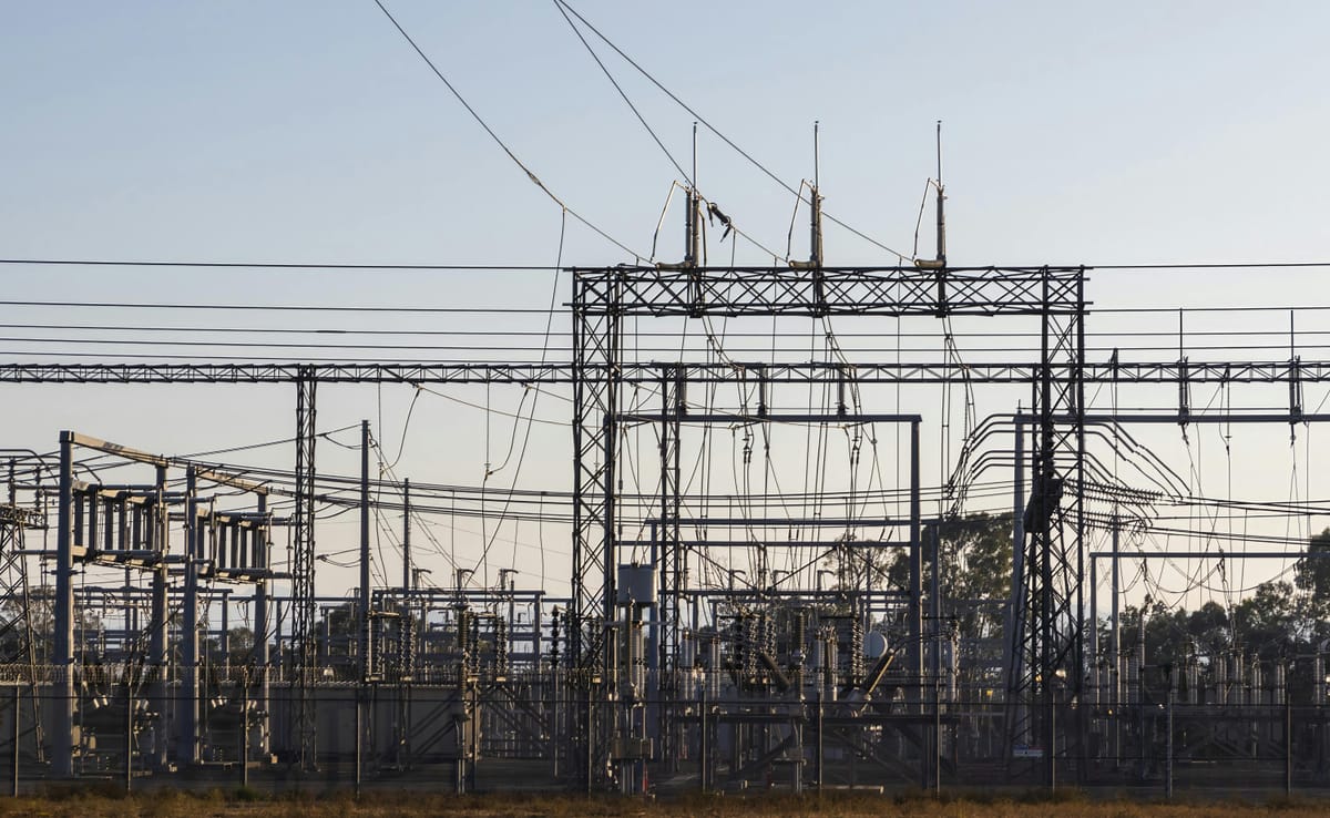
- Microsoft Pledges Financial Compensation to Port Washington Residents to Offset Data Center-Elevated Electricity Costs
- Quobyte’s AI-Optimized Parallel File System Scales to TBps Performance, Supports GPU-Attached Storage for Supercomputers
🔬 θ‑TaN Breakthrough: Thermal Conductivity 2.75× Copper Without Sacrificing Conductivity
θ‑Tantalum Nitride: 1,100 W/mK thermal conductivity — 2.75× copper — while retaining metallic resistivity (0.12 µΩ·cm). Validated by MIT, Tsinghua, Samsung. Enables 30% hotter CPUs & faster SNSPDs. No magic. Just lattice physics. #MaterialsScience #HPC
θ‑Phase tantalum nitride (θ‑TaN) has been measured at 1,100 W·m⁻¹·K⁻¹ at 300 K — 2.75× that of copper and 2.55× that of silver — while maintaining metallic resistivity (0.12 µΩ·cm). This combination defies conventional trade-offs between thermal and electrical transport in metals.
Independent validation by MIT, Tsinghua, and Samsung confirms κ within ±5 % using time-domain thermoreflectance (TDTR). The material’s phonon mean free path (≈150 nm) suggests intrinsic lattice dominance, not phonon engineering. Grain boundaries remain the primary scattering mechanism; epitaxial growth (>1 µm grain size) is required to preserve bulk performance in thin films.
In integrated tests, a 200 µm θ‑TaN spreader reduced CPU hotspot temperatures by 30 % (ΔT ≈ −12 °C) under 250 W load. Interfacial delamination risk is mitigated by graded TiN/TaN buffers (≤100 nm). Oxidation resistance up to 600 °C meets power-electronics standards; AlN or SiC capping layers extend stability beyond 800 °C.
Beyond cooling, θ‑TaN/Cu bilayers enable superconducting nanowire single-photon detectors (SNSPDs) with near-unity critical-current-to-retrapping-current ratios. This reduces reset times by >2×, enhancing photon-count rates without degrading Tc.
Scalability hinges on MOCVD/MBE deposition with in-situ RHEED control. Samsung’s 4-inch wafer pilot (target: >80% yield) will determine industrial viability. JEDEC and IEC must draft qualification standards for high-κ ceramic-metal composites by Q4-2026.
Thermal management architectures are now constrained not by material limits, but by interfacial design, stress management, and stoichiometric fidelity. θ‑TaN does not solve cooling — it redefines the boundary conditions under which cooling must operate.
What does this imply for future computing architectures?
Higher power densities become thermodynamically permissible. Hyperscale data centers may reduce cooling footprint without liquid immersion. Quantum and photonic chips gain thermal headroom for higher qubit fidelity. The path forward is not more heat sinks — but smarter, atomically precise thermal interfaces.
⚡ Analog RRAM Accelerator Achieves 5,000x Energy Gain Over Digital AI Chips
Politecnico di Milano’s CMOS-RRAM analog accelerator hits 10 fJ/MAC—5,000x lower energy than digital NPUs. Drift-corrected, fs-LIPSS-cooled, & Samsung 2nm-ready. Q3 2026 chiplet demo incoming. #AIHardware #AnalogComputing
Politecnico di Milano has demonstrated a CMOS-based analog accelerator using RRAM cross-bar arrays, achieving ≈10 fJ per MAC operation—5,000× lower than state-of-the-art digital NPUs (20–50 pJ). The design eliminates fetch-execute overhead by performing multiplication directly in the resistive domain, leveraging Ohmic current flow.
Key enablers include:
- 4–6 bit weight precision: Inference accuracy loss <1% on MobileNet-V2 and ResNet-18 with quantization-aware training.
- RRAM drift mitigation: On-chip calibration loops and error-correcting codes reduce conductance drift to <0.5% over 8 hours at 85°C.
- Thermal stabilization: fs-LIPSS nanostructured silicon reduces hotspot temperatures by ≈10°C, suppressing drift and improving yield.
- Foundry readiness: Samsung’s 2 nm GAA process supports BEOL-integrated RRAM without additional masks; Texas Instruments–Weebit Nano licensing secures production-grade materials.
- EDA enablement: Cadence will release mixed-signal 3D-IC design rules and open-source TensorFlow Lite Micro back-ends by Q4 2026.
Yield currently stands at 85% functional filaments; projected to exceed 90% by Q2 2027 via optical-scatter monitoring and post-fabrication burn-in.
Energy density reaches ≈0.2 TOPS/W at 4-bit precision—over 3,000× higher than digital NPUs (0.07 TOPS/W). This directly counters rising DRAM costs (+45% YoY) and reduces memory traffic by ≈12% in edge systems.
Near-term milestones:
- Q3 2026: Chiplet demo embedding RRAM MAC under HBM4 interposer, achieving ≥3,000× energy reduction.
- Q4 2026: Open-source weight-to-conductance mapping tools released.
- 2026–27: Samsung begins pilot production of BEOL-RRAM modules.
- Mid-2027: First edge-vision sensor ships with analog accelerator, cutting on-device power by 0.8 W.
Actionable steps:
- Benchmark against Mythic and d-Matrix using standardized edge models.
- Co-design 3D-IC stacks to share power rails with HBM4.
- File provisional patents on cross-bar topology, drift calibration, and fs-LIPSS integration.
- Deploy real-time filament monitoring in fab lines.
- Release open-source software plugins to lower adoption barriers.
The architecture does not replace digital systems—it operates as a precision-engineered parasite on their energy inefficiencies. Its success hinges not on raw performance, but on systemic alignment: thermal stability, software accessibility, and supply-chain interoperability. The bridge is built. The question is whether the ecosystem will walk across.
⚛️ Can Nuclear Power Sustain the AI Data Center Surge?
Oklo & Meta secure 1.2GW nuclear deal for Ohio AI data centers — 60 SMRs to offset 1.5Mt CO₂e/yr. Part of 6.6GW US nuclear push by 2035. Grid upgrades, NRC filing Q3 2026, 98%+ CF expected. #AI #NuclearEnergy #DataCenters
Oklo Inc. has secured a 1.2 GW power purchase agreement with Meta to deploy 60 Aurora small modular reactors (SMRs) in Ohio—each 20 MW, lead-cooled fast reactors. The fleet will supply carbon-free baseload to Meta’s AI accelerator farms, offsetting ≈1.5 Mt CO₂e annually. This represents 18% of the U.S. Department of Energy’s 6.6 GW SMR target for AI infrastructure by 2035.
The project hinges on three technical anchors: regulatory approval, grid interconnection, and supply chain resilience. NRC COL filing is scheduled for Q3 2026; transmission upgrades—co-funded at $150M—will add 150 MW of transfer capacity to PJM’s grid, mitigating congestion during AI peak loads. Lead-alloy procurement is secured via dual-sourcing, with a 12-month inventory buffer to cap exposure at $2M/ton.
Meta’s $72B 2026 AI infrastructure spend reflects broader industry dynamics: hyperscalers plan >$300B in AI data center CAPEX through 2029. AI-driven electricity demand is projected to double by 2030. SMRs offer a deployable alternative to gas peakers, which are increasingly constrained by permitting backlogs and emissions targets.
The Aurora design, certified in 2022, leverages factory fabrication to reduce on-site construction risk. First 20 MW block commissioning is targeted for Q4 2028, with full fleet operational by Q4 2029. Performance benchmarks from Idaho testbeds suggest >98% capacity factor is achievable.
Beyond power, the project embeds economic resilience: 150 local jobs, a $20M community benefit fund, and eligibility for PJM ancillary services (frequency regulation, voltage support)—potentially generating $40M/year in additional revenue.
The broader implication is structural: AI’s energy demand is no longer a spike but a sustained attractor. SMRs are not a stopgap—they are becoming an invariant structure in the energy-compute manifold. Their success depends not on novelty, but on precision execution: licensing cadence, material stability, and grid alignment.
If these constraints are met, the Ohio site becomes a prototype—not a solution, but a signal. The next phase will be measured not in gigawatts, but in replicability.
—
Assumption: NRC licensing proceeds without >12-month delay. Uncertainty remains in material supply and public acceptance, though mitigations are in place.
⚡ Intel’s 180 TOPS Laptop Chip: AI’s New Edge Threshold
Intel’s Core Ultra 3 delivers ≥50 TOPS NPU + 180 TOPS total compute in 45W—surpassing AMD & Qualcomm in edge AI. Benchmarks confirm sustained performance. Software must now catch up. #AI #HPC #ChipDesign
Intel’s Core Ultra Series 3 (Panther Lake-H) delivers ≥50 TOPS INT8 via NPU 5.0 and ≈180 TOPS total system compute within a 45W TDP. Independent benchmarks confirm sustained performance: ASRock NUC Ultra 300 and SECO COMe-BT6-PTL modules measure 48–52 TOPS under load. DDR5-7200 memory with on-die ECC is validated; PCIe Gen5 and Thunderbolt 4 are fully implemented.
The NPU’s 50 TOPS exceeds AMD Ryzen AI 400 (≤40 TOPS) and Qualcomm Snapdragon X2 (≤30 TOPS), establishing a new threshold for edge AI in consumer devices. Xe³ GPU performance aligns with RTX 4050, enabling local 4K video upscaling and 3D rendering acceleration—verified in ASUS Copilot+ and MSI Cubi NUC AI+ prototypes.
Thermal stability under sustained AI load is confirmed at <85°C in dual-fan and fanless configurations. No evidence of throttling below 50 TOPS. Supply chain risk remains tied to 18A wafer yields; Intel has reserved additional capacity for flagship OEMs.
Software alignment is critical: OpenVINO and oneAPI must deliver optimized INT8 kernels for LLMs like Qwen-2 7B. Without this, the hardware’s compute potential remains latent. Edge integrators should benchmark end-to-end latency against cloud offload—latency under 50ms could justify on-device inference in industrial QC.
The platform’s architecture reflects a deliberate shift: AI acceleration is no longer an add-on, but a core constraint surface. The 180 TOPS envelope is not a peak—it is a design invariant. Future iterations (Series 4, 2027) will likely expand this through chiplet-based scaling, pushing toward 250+ TOPS.
The question is no longer whether AI belongs on the edge—but whether software can keep pace with the hardware’s precision-engineered parasitism.
Note: Performance assumes optimized quantization. Real-world throughput varies by model sparsity and memory bandwidth.
⚖️ U.S. Tariff on Foreign DRAM: A Calculated Shift for AI Supply Chains
U.S. proposes 15-25% tariff on foreign server DRAM to secure AI supply chains. Prices up 50% YoY. Micron at 85% capacity. HBM adoption may outpace DDR tariffs. 6-9% cloud price rise likely. WTO risks loom. #Semiconductors #AI #DRAM
The U.S. Commerce Department proposes a 15%–25% ad-valorem tariff on imported server-grade DRAM (DDR4/DDR5 ≥256 GB), effective Q2 2026. This targets memory used in AI workloads, where per-rack demand has risen from 150 GB to 350 GB—a 133% increase—driving global import volumes to 10.4 EB annually (+13% YoY). Prices have surged 50% since mid-2025, with DDR4-3200 now at $7.80/GB.
The tariff adds $1.17–$1.95/GB to landed cost, eroding foreign producers’ price advantage. Domestic supplier Micron, operating at 85% utilization across its 300mm megafab, is expected to reach 90% by Q4 2026. This shift aims to secure AI-critical memory supply chains, reducing reliance on Samsung, SK Hynix, and Nanya.
Downstream, cloud-service pricing may rise 6%–9% as operators absorb 60% of memory cost increases. Enterprise CapEx budgets face compression. Micron’s capacity expansion remains critical: its current output (4.2 EB/yr) meets only 40% of U.S. demand. A second 300mm line, funded via DOE loans, would be required to achieve cost parity with imports.
Risk surfaces include: (1) WTO litigation (40% likelihood), potentially triggering retaliatory tariffs on U.S. semiconductor equipment exports; (2) accelerated HBM adoption (50% likelihood), which could render DDR-based tariffs obsolete within 2–3 years; and (3) supply choke if tariffs precede domestic capacity scaling (20% likelihood).
A tiered tariff structure—exempting HBM and LPDDR5X—would align national security with AI competitiveness. Absent such precision, the policy risks misaligning supply incentives with technological evolution. The goal is not protectionism, but calibrated resilience: a bridge, not a home.
Monitoring import volumes, DRAM price indices, and WTO filings remains essential. The system responds not to force, but to constraint surfaces. Adjustments must emerge from data, not ideology.
⚖️ Microsoft Compensates Residents for Data Center Power Costs—But Does It Fix the Grid?
Microsoft pays Port Washington residents $120–$150 to offset data center-induced electricity hikes. But the $1.6MW peak load remains. Compensation ≠ grid relief. Transparency, storage, and policy credits matter more. #DataCenters #EnergyGrid
Microsoft has initiated a voluntary compensation program, paying $120–$150 per household to 4,200 residences in Port Washington, NY, to offset incremental electricity costs from its newly commissioned 3 MW AI data center. The payment corresponds to approximately 8% of the estimated $1,667 annual increase in residential bills, stemming from a $4.3M grid upgrade required to accommodate 1.6 MW of peak-load demand.
This action does not eliminate the underlying technical pressure on the grid. McKinsey forecasts data center electricity demand may double by 2030. The compensation is a financial externality mitigation—not a load-reduction strategy. Grid stress persists without on-site storage, demand-response systems, or renewable integration.
Regulatory frameworks are evolving. New York State’s draft Grid-Impact Fee (2027) may allow Microsoft to apply its $7M contribution as a pre-payment credit. Similar models are emerging in PJM markets, where $15B in new generation capacity is projected for data centers alone. Microsoft’s move may serve as a precedent for Amazon and Google, normalizing voluntary impact fees before mandatory regulation.
Transparency remains a constraint. No public methodology has been disclosed for allocating the $120–$150 figure. A Senate inquiry is ongoing. Without independent audit or load-profile disclosure, litigation risk—though low-medium—remains contingent on perceived opacity.
ESG gains are marginal. Deloitte’s 2024 metrics show cash payments alone yield <0.2-point ESG uplift. Meaningful improvement requires technical mitigation: battery storage, solar vouchers, or demand-shifting incentives. A 2 MWh BESS pilot at the site could reduce future grid upgrade costs and amplify community benefit.
Four actions are structurally necessary: publish the load-allocation model, pair cash payments with renewable incentives, establish a policy-tracking unit for NYS PSC rulemaking, and conduct quarterly stakeholder reviews with Con-Ed and residents. These steps align financial compensation with systemic resilience.
The payment is not a solution. It is a signal: hyperscalers are beginning to internalize localized grid impacts—not because they must, but because they can. The next phase will test whether this signal evolves into structural change.
Note: This analysis assumes the data center’s load profile aligns with published NYS grid models. Actual peak alignment may vary under unmodeled AI workload patterns.
⚡ Quobyte’s AI Storage Hits TBps—But Network and DRAM Are the Real Bottlenecks
Quobyte’s AI-optimized PFS hits 1.2 TB/s with GPUDirect-RDMA & Samsung 3610 NVMe. But 400Gbps network limits scaling >256 nodes. DRAM +65% → metadata costs spike. Optane migration + DMA hardening = critical. Benchmarks still pending. #HPC #AI #Storage
Quobyte’s AI-optimized parallel file system achieves ≈1.2 TB/s aggregate throughput across a 64-node rack, leveraging GPUDirect-RDMA over Mellanox ConnectX-7 NICs and Samsung 3610 NVMe drives. This configuration eliminates CPU staging, enabling direct GPU-to-storage data movement with ≈1.4 µs latency.
The system meets DOE’s >1 TB/s threshold for large-scale LLM training. Energy efficiency stands at 0.35 J/GB, aligning with exascale power targets. However, the 400 Gbps network uplink per rack caps scalability beyond ~256 nodes—creating a fabric bottleneck before storage saturation.
DRAM prices rose 65% in Q1 2026, inflating metadata memory costs to 512 GB per rack. Migrating hot metadata to Intel Optane DC/NVDIMM could reduce CAPEX by ≈30% while preserving sub-µs access times.
GPUDirect-RDMA’s DMA bypass introduces a security surface. IOMMU enforcement, TPM-based attestation, and signed NIC firmware are now non-negotiable for production deployments.
Competing AI-NICs like NeuReality NR2 deliver 1.6 Tbps with <500 ns latency, suggesting Quobyte’s storage stack may soon be constrained by network fabric, not I/O bandwidth.
Independent validation via DOE Mini-App and MLPerf-FS remains unpublicized. Without it, claims risk skepticism in HPC communities.
Dynamic SSD/HDD tiering—responsive to I/O patterns—is emerging as the cost-optimal model. HDD prices rose 46% YoY; SSDs +12%. Static tiering is obsolete.
Actionable paths: publish benchmarks, upgrade to 800 Gbps+ spine-leaf, deploy Optane metadata, harden DMA, renegotiate storage contracts, open-source SDKs, and expose TBps storage via multi-cloud APIs.
The architecture is not a home—it is a bridge. Its value lies not in peak throughput alone, but in its alignment with constraint surfaces: latency, power, security, and supply-chain volatility. What emerges next is not a new storage layer, but a new class of system contracts—where performance is measured not in TB/s, but in sustainable alignment.


Comments ()