China Drafts AI Companion Rules with 2-Hour Reminders, U.S. Influence, and Global Compliance Shifts Amid NVIDIA Feynman

TL;DR
- SK Telecom unveils A.X K1, South Korea’s first 519B-parameter AI model optimized for Korean language, enabling teacher-model knowledge distillation to smaller models
- LG Electronics launches DQ-C2 in-house AI semiconductor with enhanced CPU and memory, enabling complex AI computations in smart home appliances
- China's Cyberspace Administration proposes draft rules requiring AI companions to remind users every 2 hours they're interacting with AI, banning emotional manipulation and minors exposure
- NVIDIA plans to dominate AI inference with Feynman chips using hybrid bonding and SRAM stacks, integrating LPU units to reduce memory latency and energy consumption
- TSMC confirms 2nm wafer capacity fully booked through 2026, with 3% price hike effective January 2026 as Apple secures majority of initial supply
China’s AI Companion Draft Rules: 2-Hour Reminders, Minor Protections, and Global Compliance Shifts
China’s Cyberspace Administration (CAC) has introduced draft rules for AI companions—requiring 2-hour reminders, banning emotional manipulation, and tightening minor exposure. With 515 million generative AI users (including 45.8% of university students), the regulations aim to balance innovation with safety as the sector surges.
What Do the Draft Rules Specifically Require?
- Mandatory 2-hour reminders for AI companion users.
- Ban on emotional manipulation tactics.
- Age verification for minors, with 3-hour reminders and prohibitions on impersonating sexual/health professionals.
- Public comment period: Dec 28, 2025–Jan 25, 2026; civil penalties: US$1,000–1,500 per violation.
Why Target Minors and Emotional Manipulation?
China’s 515 million generative AI users include 45.8% university students, a group vulnerable to addictive interactions per JAMA Network Open studies (May 2025). The rules create a "digital guardianship" layer, aligning with global concerns about AI persuading children.
How Do China’s Rules Compare to Global Models?
The CAC cites California’s SB 243 (enacted Oct 2025, 3-hour minor reminders) as a precedent—showing "policy diffusion" from U.S. sub-national to Chinese national regulation. Both use time-based prompts to reduce covert engagement, pushing multinationals (Google, OpenAI) toward unified Asia-Pacific/North America compliance.
What Impact Will This Have on AI Firms?
- Product Redesign: UI timers and labeling will raise engineering costs by 5–10% (based on comparable implementations).
- IPO Timing: Compliant firms (Z.ai, Minimax, Zh.ai) could list on the Hong Kong Stock Exchange by Jan 25, attracting US$200–300 million.
- Legal Exposure: Firms with >10 million users face over US$10 million annual liability if non-compliant.
Could This Signal Global AI Safety Norms?
The CAC’s rules are China’s first comprehensive national policy on anthropomorphic AI, merging user awareness with behavioral safeguards. The policy echo between China and California suggests emerging global norms, forcing cross-border firms to adopt harmonized compliance to mitigate risk.
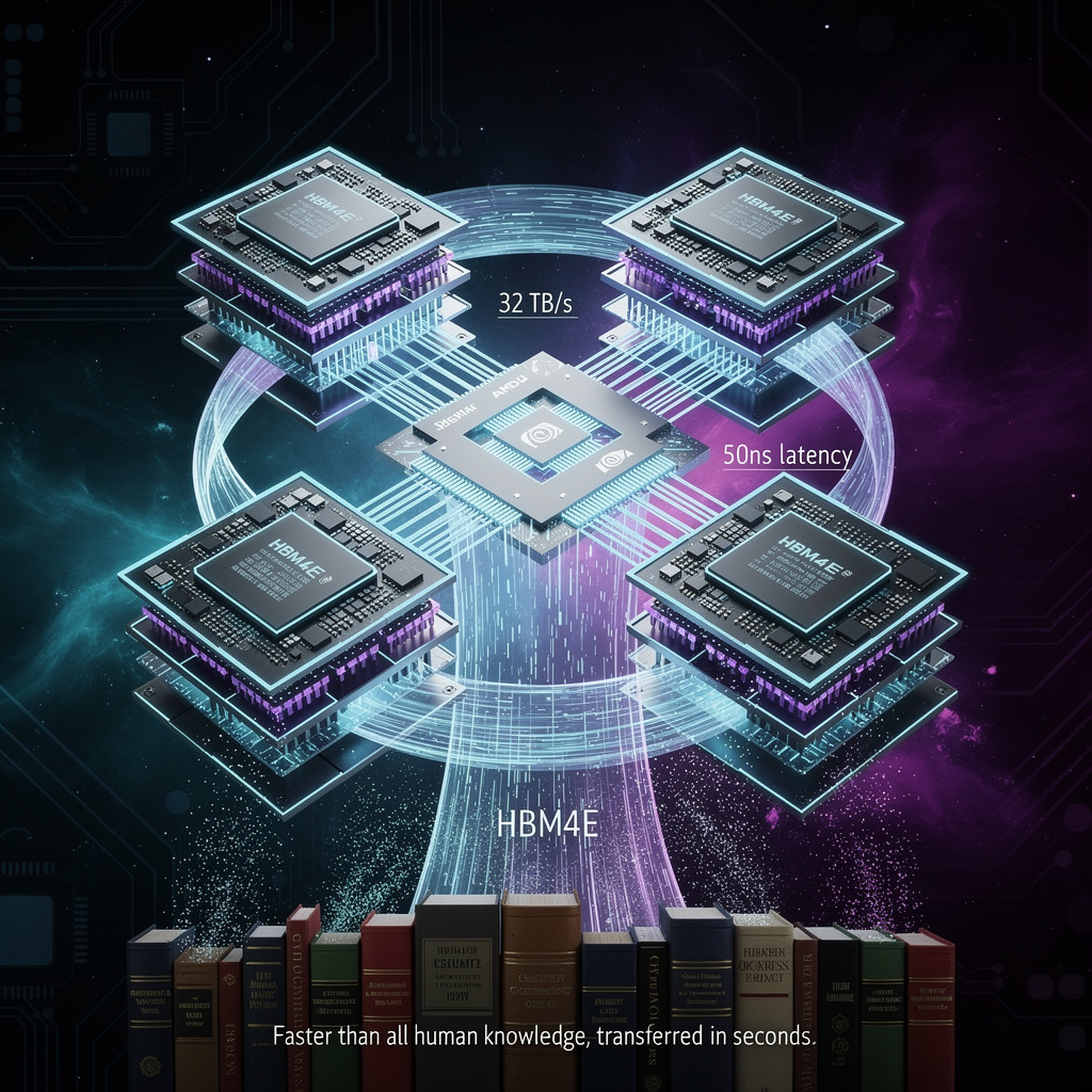
NVIDIA Feynman Chips: Can Hybrid Bonding & LPUs Dominate AI Inference?
NVIDIA’s Feynman chip lineup targets AI inference dominance via hybrid-bonded SRAM stacks, stacked LPUs, and TSMC’s 1.6nm process—all aimed at slashing latency and energy use. Can these technical bets deliver sustained market leadership?
What Technical Innovations Underpin Feynman’s Strategy?
- Hybrid-bonded SRAM stacks: TSMC’s SoIC packaging integrates SRAM dies onto the compute die, delivering ~200MB on-die SRAM with ≤0.5pJ/bit energy, 30% lower latency than HBM-3E, and less off-package bandwidth pressure.
- Stacked LPUs: Dedicated inference-only compute units above the main die handle token-wise matrix multiplies and KV-cache lookups, cutting power by 30% for transformer decode and boosting QPS by 2–3× at constant TDP.
- 1.6nm A16 process: TSMC’s node doubles tensor-core density vs. Ada/Blackwell, enabling >2 TOPS/mm² FP16 throughput and >10k QPS for Llama-2-70B on a single GPU.
- FP8/FP4 quantisation: Native support compresses 70B-parameter model weights to ~7GB, halving VRAM demand and letting 32GB GPUs host >100B-parameter models with on-die SRAM buffering.
How Do Market Trends Boost Feynman’s Edge?
- AMD X3D 2025: NVIDIA mirrors SoIC packaging but adds inference-specific LPUs, positioning it as the only vendor with both high-density compute and dedicated inference pipelines in one package.
- Groq licensing: Absorbing Groq’s SRAM-centric LPU concepts accelerated development; benchmarks show 4.2× faster single-token latency than baseline GPU kernels.
- HBM3E/HBM4 shortages: Hybrid SRAM reduces reliance on expensive HBM, cutting GPU BOM costs by 6% and mitigating supply chain exposure.
- Memory price volatility: On-die SRAM diminishes need for external DRAM buffers, improving cost predictability for cloud providers.
- MoE scaling: LPU SRAM caches active expert weights, boosting MoE model throughput by 6–10% without extra silicon.
What Data Supports Feynman’s Cost Claims?
- Hybrid bonding adoption: NVIDIA and AMD’s SoIC success means >70% of new AI inference ASICs could use package-level memory by H2 2026.
- Energy reduction: Feynman LPUs could cut data-center inference energy per token from 0.45J to ≤0.30J by 2026–27 (per NVIDIA/Groq benchmarks).
- VRAM savings: FP8 native compute enables 70B-parameter LLMs on 32GB GPUs, expanding edge use cases.
- Supply chain risk: TSMC SoIC capacity constraints may delay mass production to Q1 2026, but long-term contracts mitigate this.
What Risks Could Halt Feynman’s Dominance?
- Yield loss: 1.6nm node + 3D bonding complexity mitigated by redundant SRAM banks, aggressive binning, and test-chip feedback.
- Software lag: CUDA 12.5 (Q1 2026) includes LPU-optimized libraries (cuBLAS-LPU, cuDNN-LPU) to address ecosystem gaps.
- SoIC capacity: Shared demand from AMD/NVIDIA may delay Feynman to Q1 2026, but long-term wafer contracts with TSMC help.
- Regulatory limits: US-China export controls restrict Feynman, but H200-class GPUs ship under approved licenses.
What’s the Feynman Rollout Timeline?
- Q2 2026: Pilot tape-out with full SRAM-LPU stack; early adopters (Google, Microsoft) achieve 20% lower inference TCO.
- Q4 2026: First-gen Feynman ships to cloud providers; data-center QPS up 45% for LLM serve, power-per-token down 33%.
- H1 2027: Feynman-L2 with 400MB SRAM and 2-stage LPUs; 100B-parameter MoE models with <10ms first-token latency.
- H2 2027: On-die FP8/FP4 dynamic scaling; 30% more VRAM savings, enabling sub-10W edge AI boxes.
Conclusion
NVIDIA’s Feynman strategy relies on technical integration and market timing—amplified by trends like HBM shortages and MoE scaling. Risks (yield, capacity) exist, but mitigations (CUDA updates, TSMC contracts) are in place. By 2028, on-track execution could secure >55% of the AI inference market—though AMD’s LPU efforts or SoIC exclusivity might narrow that lead. Stakeholders should align with Q2 2026 pilot timelines and invest in LPU-aware software to leverage Feynman’s potential.


Comments ()